Best Complete Guide to Vias in PCB Design
2022-10-10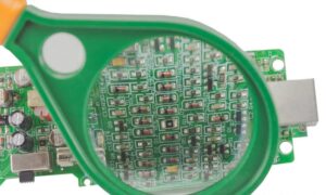
With the progressive miniaturization of electronics, surface mount technology has become increasingly popular. Essentially, vias are small vias that pass through a PCB laminate. Vias are essential in multilayer boards because they create connection paths between different layers of the printed circuit board.
What are the types of PCB through-vias?
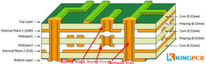
Depending on the needs of the application, as well as the location of the vias in the stack and the number of layers they pass through, the commonly used vias can be divided into three types.
- Through vias
Through vias indicate that they pass through all layers of the PCB and are open at the top and bottom layers of the board. They usually have a larger size than other types of vias. It was the most common and most commonly used.
- Buried vias
Buried vias, as the name implies, are vias buried in the inner layers of the board, not connected to the outer layers, and are commonly found in multilayer PCBs. It is useful for reducing the PCB aspect ratio (PCB thickness to through-via diameter ratio is also very useful)
- Blind vias
These vias start from the outer layer of the board and go through one or more inner layers, but are not connected to the other side, while through vias connect both sides of the board. Blind vias are useful for increasing the number of connections between the internal and external layers, effectively reducing the number of alignments and increasing the efficiency of the PCB's use.
Other vias in the PCB
- Vias in pad
Along with the move to higher integration densities for electronic components, this also means an increase in the number of interconnect pins. Designers use vias applied directly to BGA (ball grid array) pads, also known as vias in the pads, in their designs. It reduces the space needed to use the PCB, resulting in a smaller board. However, vias in pad may cause the vias to fill up during the soldering process, making them unusable.
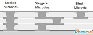
- Laser Microvia
Microvias are the smallest through-vias, typically about 0.003" - 0.004" in diameter (equal to or less than 150 µm). It was explicitly used in boards with many interconnects(HDI PCBs). The aspect ratio of micro vias is 1. It requires laser equipment to drill through holes, which is relatively costly.
- Thermal vias
Thermal vias are used to conduct heat to the back side of the PCB by using the perforations of the PCB. Active components, high performance microprocessors and high frequency components generate a lot of heat. In order to dissipate heat effectively, the thermal vias must be placed as close as possible to the component generating the heat.
How do I determine the correct vias for my PCB?
There is a strong relationship between the type of through-hole and the size and function of the board. In larger devices with boards, PCBs with through-vias components may be more efficient. On the other hand, for smaller devices, micro-blind vias work best, but the investment cost may be relatively high.
When you communicate with your manufacturer, you must clearly state your through-hole requirements in the manufacturing documentation, preferably using a separate document stating the through-hole requirements.
To sum up
The popularity of miniaturized and high-density designs for appliances has made through-holes increasingly important, and their role is
- Increase board alignment density
- Aids in signal transmission between different layers
- Helps build component density
Contact Us
KingPCB has over 10 years of experience in PCB manufacturing and assembly in China, not only for conventional circuit board manufacturing, but also for providing high precision multilayer PCB vias.
Our quick response, high quality manufacturing, and timely delivery capabilities set us apart from other manufacturers. If you have any questions or would like a quote for your project, please feel free to contact us via email!
