HDI PCB
HDI PCB
Get quotation for your HDI PCB,welcome to contact us at Sales@kingpcb.com
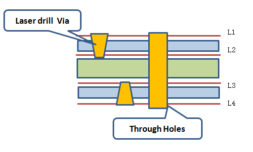
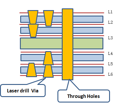
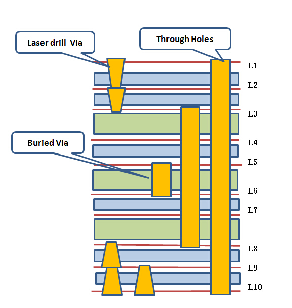
The full name of HDI is High-Density Inter-connector, it is a kind of technology (technical) for producing printed circuit boards, it uses a micro-blind buried hole technology to provide a circuit board with a relatively high distribution density, HDI is a compact product designed for small-volume users.
For the electrical requirements of high-speed signals, the circuit board must be provided with an alternating current impedance control, high frequency transmission capability, etc,multi-layering becomes a necessary design.In order to reduce the quality problem of signal transmission, and in order to cooperate with the miniaturization an array of electronic components, the circuit board are also constantly increasing its density to meet the demand, the emergence of assembly methods for BGA and other components has pushed printed circuit boards to an unprecedented high-density realm.
While electronic design continues to improve the performance of the whole machine, it is also trying to reduce its size. From small mobile phones to small portable products with smart products, "small" is the constant pursuit. HDI technology can make the terminal product design more compact. at the same time meet the higher standards of electronic performance and efficiency, HDI PCB are now widely used.
Advantages of HDI PCB:increased line density is conducive to the use of advanced construction technology,better electrical performance and signal accuracy,better reliability,improved thermal properties, improved RF interference / electromagnetic interference / electrostatic discharge (RFI / EMI / ESD ), increase design efficiency, etc.
Welcome To Start Your Business Now!
Contact Us