What is the Best Test Points in the PCB?How to Use Them?
2022-12-09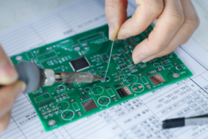
As a testable design (DFT) method, test points simplify the PCB testing process. The process that takes place in the later stages of production can be effectively improved by creating PCB test sites to test the specifications and weldability of the components on the board.
What is a test spot on a PCB?
ICT (In-Circuit-Test) equipment is generally used for PCB measurement. It uses Bed-Of-Nails to touch all parts of the board that need to be measured for the test.
A PCB test point is a small loop of wire used to test a probe on a PCB containing surface mount components. They enable users to inject test signals or monitor circuit boards during production. Test sites come in a variety of materials, sizes and colors.
The PCB test point provides a location for the J-hook, or has a sharp tip to contact the conductor on the plate. Most surface mount test sites use phosphor bronze alloys, but they can also be coated with a more affordable silver coating.
What are the advantages of adding test points to your PCB?
Implementing test points in PCB design will provide the following benefits during development:
- Time and cost savings:
By detecting connection problems through test points in the early design phase, you can save time and money in the later phases.
- Test convenience:
Test points offer a much lower configuration than other test probe connection types. The shape of the test point is similar to that of the surface mount element, making it a more versatile option.
- Easy error detection:
Test points simplify the probe testing process, making it easier to detect potential problems.
How to design a PCB with test points?
The following factors should be considered for the correct placement of test points:
- Board side:
Typically, placing all test points on the same side of the PCB simplifies the testing process, thus saving time and money.
- Test point distribution:
By evenly distributing test points throughout the PCB, you can test with multiple probes more easily.
- High Component area:
Specifying PCB areas for high components can also simplify the testing process.
- Minimum test point distance:
PCB test points should be at least 0.100 inches apart to improve test efficiency.
- Manufacturing tolerances:
Consider manufacturing tolerances when creating the initial layout of the PCB. During the test phase, the PCB needs space to accommodate the test points and probes.
Choose KingPCB to be your PCB supplier
At KingPCB, whether it is mass production, prototyping, proofing services, we have the confidence to complete any of your PCB manufacturing and assembly needs!
Contact us now for a free quote on your project.
Prev: What is PCB OUTGASSING?
Next: PCB Corrosion Causes
