Concise Analysis of the Flexible PCB Manufacturer’s Manufacturing Process
2020-03-06Flexible PCB Manufacture: Simple Analysis of the Manufacturing Process
Flexible PCB manufacturers understand that modern technology requires enhanced and sophisticated Printed Circuit boards. Therefore, they are investing immense time in designing and developing state of the art Printed Circuit Boards.
The modern technology demands the continuous expansion of Flexible PCB. Over the years, we have seen tremendous growth in terms of flexible PCB application scope and application field. In addition, the prospect of development of both national and international markets further enhances its importance.
It seems that in no time, Flexible Printed Circuit boards will be as important complex and complicated as the rigid printed boards. There will be a significant improvement in terms of structure, types, verities, and grades.
In the course of this article, we are going to present you with a simple analysis of the flexible Printed Circuit Board’s manufacturing process. So, without any further delays, let us get straight to it.
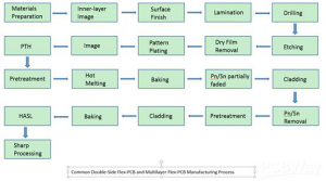
Manufacturing Process of Flexible Printed Circuit Board
The picture below shows the manufacturing process of Multilayer FLEX-PCB along with the Common Double-Side Flex Printed Circuit Board.
Blanking: Material Preparation - Flexible PCB Manufacturer
The first step in the manufacturing process is the preparation of the material, blanking. This step mainly includes reinforcing pate, cladding layer, and flexible copper clad laminate. Likewise, the separation of the main auxiliary materials that the manufacturer uses for lamination takes place in this step.
Then comes silicon rubber plate, or conformal material, absorption of the in, coated paper among others.
Drilling - Flexible PCB Manufacturer
Drilling requires attention and effort. Regardless of the material, may it be cladding layer or the copper-clad laminate, It is difficult to drill them. Yes, they are soft and thin, yet accurate drilling is challenging.
A good idea is to stack boards before you drill. You stack-up multiple pieces of copper clad laminate or cladding layer before you drill them. Put them on top of each as you would put the books.
Pitting and Desmear - Flexible PCB Manufacturer
After the drilling process, some sort of dirt might accumulate in the PCB holes. Thus, you need to clean these holes properly. To ensure the quality of the plated-through role, it is imperative to keep the holes completely dust-free.
For the double-sided copper-clad laminate, it is critical to do the desmear and pitting. Only after that should you carry out the PTH.
PTH and Pattern Platting
First comes then desmear and pitting, then you have the electroless plating, after then comes electrical plating, imaging and finally pattern plating.
Electroless Plating
Electroless Plating pretreatment solution should be alkaline ionic palladium instead of the acidic colloid palladium. The alkaline would generate better and more refined results.
Also, the important thing here is to ensure that both speed and the reaction time needs to be kept in check. Make sure that the is not very fast nor is it takes too long for the reaction time. In case both of these factors do not have a balance, it will lead to multiple holes. Thus, the flexible PCB manufacturers will end up with the copper layer’s poor mechanical properties.
Electrical Plating: Flexible PCB Manufacturer
If the flexible PCB ends up with poor mechanical properties, for instance, the ductility, it will not offer robustness. The electroless copper plating layer might not be able to withstand the thermal shock and it will end up being broke or damaged.
So, a good rule of thumb is to carry out the electrical plating immediately after the copper plating layer reaches up to 0.3~0.5um. When you instantly carry out the electrical plating, it would thicken the entire panel to 3-4um. Thus, it will make the hole sturdy and strong. The integrity of the holes will remain intact in the proceeding processing steps.
Pre-cleaning and Imaging
Pre-cleaning is a prerequisite for the imaging. The flexible PCB manufacturer ensures that a proper cleaning takes place before they go on imaging the Printed Circuit Board.
There is no difference between the pre-cleaning process of the rigid PCB and the Flexible PCB. One of the major reasons for using electrolytic cleaning process or chemical cleaning process for a flexible substrate is because it easily bends and deforms.
The process also uses either the special pumice stone paint or manual pumice board machine Another thing that is similar to the right PCB is the process of exposure and developing along with the process of sticking the dry film.
Once the polymerization reaction takes place, there is a visible difference between the then binding force of the copper foil. The dry film becomes brittle due to developing and this results in the decrease of copper foil’s binding force. Thus, after developing the dry film becomes more focused on the prevention of it from peeling and warping.
Etching - Flexible PCB Manufacturer
The flexible substrates tend to have several long parallel wires at their bend. It is imperative to pay close heed to the spraying direction of the etching solution. After all, this is going to have a direct impact on the consistency of etching.
In addition to the spraying direction, the manufacturer needs to pay heed to the pressure along with the position of the PCB. PCB’s transmission direction also holds great importance. You need to consider all these factors during the etching process.
Another important thing is to attach a rigid substrate in front of the flexible substrate in order to full the substrate forward. To ensure better and efficient results, use the fluid automatic regeneration system for the etching of Flexible Printed Circuit Boards.
Cladding Layer Positioning
Before the cladding layer positioning becomes, it is necessary for the PCB to do the surface treatment. After etching, the binding force needs to be reinstated for the success of the cladding layer positioning.
There is a difference between the amount of moisture the flexible PCB can absorb after etching and the cladding layer after drilling. Thus, to make sure that both these materials have the same absorption level, they need to be baked for 24 hours in the drying oven.
After they are fully dried, the next step is to laminate them. In addition, the flexible PCB manufacturer should ensure that the stack height does not exceed 25mm.
Lamination
Next is lamination, it is also an important and critical step in the manufacturing of the flexible Printed Circuit Board.
Cladding Layer Lamination
The heating time, lamination time, pressure along with the value of other parameters greatly depends upon the type of flexible substrate that you use. Different flexible substrates have different values of parameters.
Below are the basic parameters of the process
- Upper Template
- Separating Film Matera
- Blotting Coated paper or paper
- Separating Film Material
- Cladding material
- Separating Film Material
- Workpiece
- Separating Film Material
- Cladding material
- Separating Film Material
- Blotting Coated paper or paper
- Separating Film Material
- Bottom Template
Key Points: Lamination time is basically the net pressure time. It should be 60 minutes under full pressure. Similarly, for the heating rate, the temperature should rise from room temperature to 173℃ in just ten or twenty minutes. The pressure should take about 5 to 8 seconds to reach 150N-300N/cm2.
Gasket Material
To ensure high-quality lamination, the flexible PCB manufacturer often chooses the gasket material. It is no doubt an excellent material. However, you need to ensure that the gasket material itself is of fine quality. It should have low fluidity, good formability, and a good cooling process.
It should not shrink, and there is no deformation. After all, the occurrence of deformation leads to bubbles in the material during the lamination. Both rigid, as well as the flexible system, contains the Gasket materials. For instance, the rigid system majorly comprises of glass cloth. To, further enhance its useability, the glass cloth is then reinforced using a good quality silicon rubber.
Flexible system on the other end includes the radiation polyethylene film or the PVC film. It also contains thermoplastic materials.
Baking Flexible PCB Manufacturer
To ensure that no moisture is left, the manufacturer needs to bake everything completely. The right time of baking will remove all the moisture.
Hot melting or HASL
To prevent the welting of the Printed Circuit board, it is imperative to carry out the hot melting or the HASL process right after the drying of PCB. If there is any delay, it can lead to a decrease in the quality of the Printed Circuit Board.
Sharp Processing
Usually, sharp processing takes place in the mass production of PCBs. For Flexible Printed Circuit Board Sharping processing is the seamless use of precision steel dyes. It can be either a multi-cavity mold or the manufacturer can use a mold a cavity.
Packing and shipping
The Flexible PCB manufacturer uses the vacuum packaging machine for the right and correct packing of flex-PCB. To extend the storage time, add a desiccant to the vacuum packaging bag. There are several ways to ship flexible Printed Circuit Boards. However, it majorly depends upon the manufacturer.
For instance, KingPCB, a leading PCB manufacturer, tends to offer several methods of shipping including DHL, FedEx and many more. You can reach out to them and they will deliver the highest quality Printed Circuit Boards at your doorstep.
