Important PCB Design points of a PCB Manufacturer in China
2020-02-16PCB Manufacturer in China: Important Points and Tips of a PCB Design
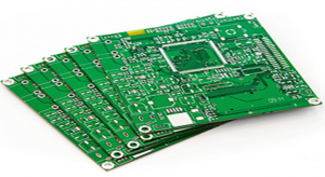
The modern PCB manufacturer in China focuses on designing and developing efficient, effective and smart Printed Circuit Boards. After all, they do understand that the design of a Printed Circuit board is going to have a direct impact on the life span and the efficiency of the product.
It is imperative for the manufacturer to ensure that a Printed Circuit Board will meet the consumer’s need for electromagnetic compatibility and the heat dissipation level. Also, the manufacturer needs to ensure that the PCB is of the right size and design. All these factors would contribute towards making an outstanding and robust Printed Circuit Board.
There are some key points and important tips for designing a Printed Circuit Board. In this article, we are going to talk about these points and tips in detail.
Table of Content
- Key Points of PCB Design
- PCB Manufacturer in China: Seven Highly Effective Tips
- Why Choose Us?
- Take Away
Key Point of a PCB Design
The first thing to measure a PCB design is to focus on its manufacturability. Having an experienced and skilled manufacturer is bound to generate better results. Therefore, you need to focus on the points below in order to ensure good manufacturability.
Key Points of Grounding Design
There are four main parts of the ground system:
- Enclosure Ground
- System Ground
- Digital Ground
- Analog Ground
It is important to consider all these four parts. In addition, a good and effective grounding design has the ability to protect most of the interference. If there is interference, it will lead to some serious problems, as shielding out the interference is imperative for the electrical equipment.
Point 1
First thing first, it is important for you to select a grounding method that is reasonable. There are two main types of grounding method namely single-point grounding technique and multi-point ground method. Both these methods are effective; however, you have to choose in accordance with the actual situation.
In case, the operating frequency of the equipment will be more than 10Mhz, then the good option is the multi-point grounding. The reason being, the higher value of the ground wire impedance has a direct influence on electromagnetic radiations. These radiations affect the normal operation of the product. If we do not keep a check on these radiations, they will hinder the normal functionality of the equipment.
In case the equipment has an operating frequency lower than 1Mhz, then the good option would be to go with a single-point ground technique. Remember, if the equipment has an operating frequency lower than 1-10Mhz, you need to decide the grounding mode by referring to ground line length and the circuit wavelength. Both of these factors will help you choose the right grounding mode.
Similarly, if the wavelength is less than about twenty times to that of the ground line length, the good option is to go with multi-point grounding. If this is not the case, then going with single-point grounding is the safer option.
Point 2
A good PCB practice is to ensure that circuits having different properties are together. You need to place circuits with different properties separately. After all, there is a high level of complexity in the circuit board’s circuit distribution.
For instance, you might come across both analogs as well as digital circuits on a single Printed Circuit Board. To ensure that there is no interface between these two circuits, you need to separate them. When you use the design of separate ground modes, you are ensuring that there is no electromagnetic interference between two or more circuits.
Point 3:
This is an important point. You need to ensure that the ground wire’s cross-section is thick and wide. It offers efficiency and reliability. If the width of the cross-section is more equal or greater to 3 mm, you can effortlessly avoid ground instability.
The instability is the reason of the change in current. In addition, it improves the anti-noise performance of any equipment. Thus, you need to choose a tick and wide grounding conductor for as long as it is possible.
PCB Manufacturer in China: Seven Highly Effective Tips
Below, we have come up with some seven most effective tips for designing a Printed Circuit Board.
Use Design to offer Flexible Application
When you are designing a Printed Circuit Board, you need to pay close heed to several factors. For instance, if you are designing a high-heat, high power, high current and high voltage Printed Circuit Board, you need to ensure that the components are loose.
Ensure that the spacing of the component pads along with each solder pin’s pad spacing to be big. Also, you can incorporate vias between the copper foil and the pads of the PCB board as per need. However, the placement of vias mainly depends on whether the size of the board and the number of circuit components allow it.
When you have some space by removing the excess PCB substrate, you improve the insulation performance between the copper foil and the components of the Printed Circuit Boards. In addition, the additional space helps in dissipating the heat among the components efficiently.
The better insulation is also useful in preventing any sort of leakage between the printed board pads and the copper foil of the PCB. Insulation also helps in preventing short circuit breakdown and burr discharge. Prevention of all these factors contributes towards a better, refined and robust Printed Circuit board.
You can determine the openings’ size and shape according to your needs. Likewise, you can also select the positions of the opening. For instance, you can choose between the copper foil of PCB, the welding feet, high power triodes, optocoupler input welding pins, optocoupler output welding pins and other required places.
Smooth Copper Foil Traces
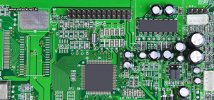
This is perhaps an imperative part of the Printed Circuit Design. All the PCB manufacturer in China ensure that the traces of copper foil are smooth. In order to do so, they make sure that the copper foil is of a small size. It is round, and chamfered, thus there are fewer burrs and sharp corners.
They ensure that it is smooth and neat and there are no lines, not even smooth ones. The main reason behind the smooth copper foil trace is the longevity of the Printed Circuit Board. A copper foil with sharp edges, having dust accumulation, burrs or moisture leads to discharge, and spark formation. This then results in short-circuiting and leakage issues.
A good practice for the emission of high-frequency signals of a radio frequency circuit board is to use a 45-degree wire in comparison to the 90 degree folded wires.
Thick and Strong Power and Ground Cables
If the manufacturer has the option, he should go with a thick and sturdy power cord as well as the copper foil ground wire. Both these wires play an important role in the performance and lifespan of the Printed Circuit Board. Thus, it is important to pay heed to them.
There are two main reasons for having high-quality ground and power cord. First, a thick ground wire is useful for improving the circuit board's anti-interference ability. It is also effective for decreasing the ground wire’s impedance. Another reason for large soldering is that the ground wire has a connection with important and large pieces of the Printed Circuit board. For instance, it connects to the metal shield plate or the ground radiator. Therefore, having a big wire can actually make a difference.
Second, a thick power cord will improve power efficiency. It is important to note here is that by adding a thin layer of tin to the surface of the copper foil, you can actually improve the circuit's functionality.
Tin incorporation will reduce the internal resistance, increase the strength of the PCB by resisting current shocks and enhance the copper foil circuit’s strength. In addition, the presence of tin act as the heat sink and it increase heat dissipation area.
Use IC Sockets
IC sockets may seem appealing, as it makes installation, removal, and replacement of the Printed Circuit Boards easier. However, a good design of Printed Circuit Boards uses limited minimal to no IC sockets. The main purpose of IC sockets is circuit designing and debugging. However, you should avoid these circuits at the beginning of the experiment.
It is possible to solder the IC directly onto the Printed Circuit Boards, but you should not do it due to its certain limitation. IC sockets and IC pins are susceptible to poor contact, thus they have an adverse impact on the circuit board’s reliability factor.
Similarly, IC socket is responsible for causing unnecessary and unwanted interference, which again leads to loss of circuit boards' reliability level. Therefore, you should not use IC sockets especially when it comes to the radio frequency circuits.
Partition Design
The design of a Printed Circuit board should be clear. It should have different parts, each part subdivided into blocks and sections based on their functionalities. So, when you divide the areas of the circuit board in accordance with their functions, you are actually enhancing its overall capacity by adding the circuit and circuit structure principle.
The proper layout will help the circuit appear orderly and neat, thus facilitating future maintenance, inspections, and eliminations.
Seismic
The PCB manufacturer in China pays close heed to the component mounting method of a Printed Circuit Board. They also closely look at the shock absorption and the seismic performance of the respective component mounting process.
It is important to focus on the installation of large components, the basic layout, circuit module components, heat dissipation conditions, high-power radiators, and interference. In addition, they need to focus on the circuit’s ability to resist vibration.
In the design, it is possible to effortlessly, increase the overall firmness of the circuit according to the component installation structure. You can reliably fix the assembly by designing additional fasteners. Doing this will enhance the stability of the circuit along with the seismic performance.
Pay attention to Ground Pad
Last, but not the least, you need to pay close attention to the design of the ground pad. Make sure that you add solder plating and small rounds to ensure reliable contact between protective lay and a thin tin, solder pads and ground pad.
To make good contact especially during the cleaning of a lace washer, you can fix the ground pad screw. The reason for Pad thinning is to ensure that the copper foil that is being exposed does not rust nor does it oxidize. In addition, it also makes the tin-plated a better, robust and reliable conductor.
Why Choose Us?
KingPCB is among the leading Printed Circuit Board manufacturers. They are known for their skills and unique PCB designs. They offer only the highest quality of Printed Circuit boards at an affordable price. The company has a steady history of clients and they are unmatched.
They use the latest techniques and technologies to design and develop outclass and excellent Printed Circuit Boards. They have highly experienced and creative staff, thus their circuit boards are unmatched.
KingPCB is the only place to shop for your PCBs, as they offer only the best. Regardless, how complex the design of your Printed Circuit Board is, they will be able to develop it without any hitches. To ensure the quality of every Printed Circuit Board, they test it individually.
After all, they firmly believe in delivering only the highest quality products. You can design and develop a small number of PCB, or you can order them an extremely large number. They will be able to handle all order sizes efficiently.
Read About: aluminum PCB manufacturer
Summary
PCB manufacturer in China follows the above design points to ensure high quality Printed Circuit Boards. They would pay close heed to the ground padding, the ground wiring, spacing, copper foil smoothness, and other similar factors to design and develop high-quality PCBs.
Their design will not incorporate the unwanted IC sockets; it will have a strong power cord and all other elements that make a PCB strong and sturdy. In short, they offer the highest quality Printed Circuit boards.
