Top Best Failure analysis techniques for PCB Assembly Manufacturer
2020-03-09PCB Assembly Manufacturer Top Failure Analysis Techniques
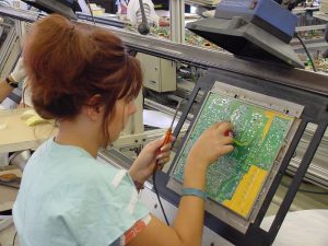
PCB assembly manufacturer understands the importance of the Printed Circuit Board. They know that PCBs are a critical part of modern electronics. Incorporating good quality PCBs into machines will ensure the quality and reliability of the equipment.
Despite this, it is difficult to avoid Printed Circuit Board failures. The PCB failures are unique in one way or the other. However, analyzing these failures can help point towards the root cause. To ensure the quality and reliability of a Printed Circuit board, you use should some failure analysis techniques.
In the course of this article, we are going to discuss some common failure analysis techniques. These techniques will help you find the root cause of the failure. They will also ensure high quality and reliable Printed Circuit Boards.
Effective Failure Technique Analysis for PCB Assembly Manufacturer
Incorporating these techniques into the production process promises high-quality, robust and reliable Printed Circuit Boards.
Appearance Inspection
This is among the most common and easy techniques for inspecting the Printed Circuit Board. You would have to visually, inspect the Printed Circuit Board with or without instruments. Magnifying glasses, metallographic microscopes, and stereo microscopes are among the few analyzing instruments.
You use these instruments to check the appearance of the Printed Circuit boards. They help you determine the parts that are causing the failure and its physical evidence. These simple, yet effective instruments help find the failures as well as discover PCB’s failure mode.
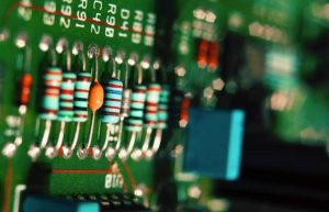
With appearance inspection, you can check the location of the explosion board, along with corrosion and pollution. In addition, the manufacturer checks the regularity of the failure along with the circuit wiring with a visual inspection.
Manufacturers often discover certain PCB failures after the PCB is assembled into a PCBA. These failures can be due to bad assembling process or due to the material. Therefore, it is imminent to carefully, inspect the material.
X-ray Fluoroscopy - PCB Assembly Manufacturer
X-ray Fluoroscopy is an excellent way to determine internal defects. Something, you might not be able to find using the visual inspection. For instance, you need to use X-ray Fluoroscopy to determine the defects of a PCB’s through holes.
X-ray Fluoroscopy technique uses different materials with different densities and thickness to absorb X-rays. It uses different principals to transmit light. In order to inspect the defects that are inside the PCB, X-ray Fluoroscopy is a good option.
It helps you find failure inside the through-holes, PCBA solder joints and the defective solder joints positioning. Initially, the X-ray Fluoroscopy used only two-dimensional imaging equipment. However, advancement has led to three-dimensional imaging and X-ray Fluoroscopy can reach below one micron.
Manufacturers now have the option of 5D equipment for packaging inspection. Nevertheless, these 5D X-ray Fluoroscopy are not only expensive, but they also have limited use in the industry. Due to these factors, they are not a good investment.
Slice Analysis
Another great PCB failure analysis technique is the Slice Analysis. Slice analysis provides you with rich and accurate information about the microstructure of the Printed Circuit Board. With Slice analysis can you gather information about the cross-section structure of a PCB.
You would use a series of methods including observation, corrosion, polishing, slicing, inlaying, and sampling to gather information. This information would act as a base to determine the quality of the next batch of PCB.
Although the method provides accurate information, yet it is destructive. After sectioning the sample, you cannot use it. You will have to destroy the sample. In addition, the techniques demand high and extensive sample preparation. These preparations take a lot of time, effort and energy. You would even need a trained technician to, successfully complete the inspection.
Scanning Acoustic Microscope
For assembly analysis and electronic packaging, PCB assembly manufacturers use an ultrasonic scanning acoustic microscope (C mode). To image the polarity, phase, and the amplitudes changes, the ultrasonic scanning equipment uses ultrasonic reflection with high frequency.
You will find the information along the XY plane and the Z-axis shows the scanning method. Thus, it is possible to determine several components and material defects using this technique. Some of the common defects include voids, inclusions, delamination, and cracks.
With sufficient width of the scanning acoustics, it is possible to determine the internal defects of the solder joints. To indicate the existence of defects, the acoustic image appearance in red instead of the usual color.
Microscopic Infrared Analysis
With microscopic infrared analysis, you can effortlessly analyze the compound composition of the material. The technique combines a microscope with an infrared spectrum. To analyze the composition, it uses infrared’s different absorption principles by different materials.
Mostly, the materials are organic substances. You can find the infinitesimal organic pollution using microscopic infrared analysis. After all, the technique combines the visible light of the microscope with infrared light within the visible field of the view.
In case, you do not combine a microscope with infrared technology, it will not be able to generate greater results. You can use the Infrared spectrum without a microscope for analyzing large sample volumes.
It is almost impossible to determine the trace pollution of a PCB. The trace pollution leads to poor solderability of the Printed Circuit Board. However, with the infrared spectrum of the microscope, you can resolve this problem.
Micro-infrared analysis’s main objective is to the cause of poor solderability and corrosion. It also focuses on finding and analyzing the surface of the joint or the organic pollutants of the welded surface.
Scanning Electron Microscope
SEM or formally known as the scanning electron microscope is the most useful and commonly used technique for conducting failure analysis. It basically is a large-scale electron microscopy imaging system. The technique offers a wealth of information regarding the Printed Circuit Boards.
It uses the anode to accelerate the beam emitted by the cathode. It then uses a magnetic lens to focus and form a beam with a diameter of several tens. The beams help creates a point-by-point scanning movement. Thus, helping you gather rich and accurate information about the Printed Circuit Board.
The technique is effective in analyzing the mechanical failure of the Printed Circuit Board or the Solder joints. It is highly efficient when it comes to analyzing the solder joint’s metallographic structure. In addition, it observes the solderable coating, measurement of intermetallic, and the surface pads’ morphology. It can even help find failure with the measurement of the tin whisker.
With SEM, you will not get a colorful image. On the contrary, the analysis technique generates a black and white image. Also, ensure that the sample of the SEM should be conductive. In case, it non-conductive, you will have to spray some carbon or gold. The same holds true for certain semiconductors.
In case, you fail to do the spray, the technique will not generate accurate results. The reason being, the accumulation of charge on the sample surface has an adverse effect on the sample observation. Moreover, the SEM image has a greater depth of field in comparison to the optical image.
Something that further enhances its outcome and overall analysis. SEM is an excellent and effective technique for uneven samples including tin whisker, microfracture and metallographic.
X-Ray Energy Spectrum
X-Ray Energy Spectrum is another excellent analysis technique that major PCB assembly manufacturer incorporate. It generates accurate and authentic information effortlessly. The method incorporates different scanning methods of the electron beam. Thus, it has the capability to perform surface point analysis along with surface and line analysis.
It can also gather information on a number of element distributions. The line analysis performs analysis of elements present on the specified line at one time. Similarly, to get all elements of a point, use the point analysis. Lastly, the surface analysis focuses on analyzing the elements that are present on a specific surface.
Photoelectron Spectroscopy XPS
In order to perform not only quantitative but also qualitative analysis of the sample surface, XPS is an excellent choice. It can conduct in-depth analysis of the shallow surface elements. Likewise, you can gather information regarding the element’s chemical valence. This information is based on the chemical shift of the binding energy.
With XPS, you can gather information regarding the surface layer’s atomic valence as well as its surrounding elements. It is possible to perform the analysis of the insulating sample without causing any sort of damage to the sample.
You can perform multiple layers of longitudinal element distribution analysis in the case of argon ion peeling. In addition, XPS allows rapid multi-element analysis as well. In short, the photoelectron spectroscopy is excellent for performing the analysis of the contamination as well as the quality of the pad coating. It is also effective for performing the oxidation degree analysis. It will help find the root cause of poor solderability.
Takeaway
PCB assembly manufacturer have been incorporating these failure analysis techniques to ensure the highest quality and reliable Printed Circuit Boards. Every analysis technique is different and is used for finding different problems.
A good manufacturer such as the KingPCB uses most of these techniques to ensure the highest quality printed circuit boards. They understand that failure in the PCB would lead to the failure of your product. Thus, they deliver only the highest quality Printed Circuit Boards.
