2021 Best Printed circuit board failure analysis Guide for Beginners
2020-12-17Practical ways to build a perfect Printed Circuit Board without errors

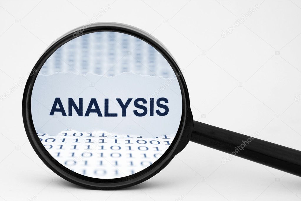
If you are scrolling to get information and techniques in order to printed circuit board failure analysis; then you are on the right page. This article will discuss the issue and flaws in the printed circuit board. Moreover, different technique to fix these flaws will come to light.
Many types of flaws can occur in the PCBs. The prominent are flaws that related to the material defects, electrical components and physical issues. These three types of flaws occur and damage the working of PCB.
Introduction to printed circuit board failure analysis
The materials present within the PCB have the specified dimensions. The semiconductors in the PCB also have the specifications in order to have exact and defined properties for the design. When the materials are not present according to the defined limit, the PCB would not work correctly.
It causes the abnormality in the function of PCB. Printed circuit board failure analysis finds out whether the certain material is present or not in the PCB design.
Due to the complex designs of the printed circuit boards, the electrical problems are numerous. The electrical problems of the PCB are difficult to eradicate and are wide spread. It takes a deep hunch and expertise to remove these flaws related to electronic components.
How do experts hold pcb failure analysis?
An effective and respective test for the electrical flaws of PCBs is to make the heat map of the entire PCB. When we implement this test, we can check the heating of all the electronic components of the PCB.
This test identifies the overheating of any component of the PCB design. This overheating is the strong indication of occurring flaw in the PCB chip. This test is a useful starting point in the printed circuit board failure analysis.
The third type of flaw occurring frequently is the physical breakdown problems. It includes the physical breakdowns related to the rust and cracks. There are many types of cracks and fractures of the PCBs.
When we find out the particular fracture in the PCB design, it is easy to check the underlying problem. This underlying problem will be the main cause to the flaw in the PCB design. The fractures and cracks may be of different varieties. They may be fatigue cracks, stress cracks and brittle cracks.
Detection Techniques for printed circuit board failure analysis
Many detection techniques are there for the identification of the flaws and problems in the PCB designs. Some of them we will discuss in this article. The electronic failure engineers use these techniques in the process of printed circuit board failure analysis.
For the detection and identification of the trace elements is the test spectroscopy. The test for the flaws and issue related to the heat traces is micro tomography. For the sake of identification of the flaws and issue relating to physical breakdown, penetrant tests are there.
The detection of the different flaws in the PCB design point out to the different techniques. The microscopy includes the many sub techniques like electron microscopy, emission microscopy and acoustic spectroscopy.
The sub techniques in the micro thermography are liquid crystal imaging and fluorescent micro thermal imaging. Acoustic microscopy is a best technique to find out the physical breakdown failures and flaws in the PCB design.
Why it is important to carry pcb failure analysis test?
In certain cases, it is difficult to find out the whole picture of the problems and flaws using one test or technique. In this situation, we implement many techniques and tests. This procedure helps us to take a whole picture of the flaws in the PCB using many techniques.
In the process of printed circuit board failure analysis, many factors participate in the detection of the flaws. These are the company of the failure analysis, the type of the analysis technique to use and the budget. In this way, the malfunctioning of the PCB can come to light without the PCB failure analysis.
A step in the identification of the failure or flaw in the PCB is the revealing the defect. This step is so critical in the analysis that it may lead to the destruction of the printed circuit board.
That is why a strong hypothesis is necessary before taking further action. The analysts use the certain points as hypothesis to select a directed course of action.
- It can lead to the potential failure of the printed circuit board. With the increase in temperature the failure is more prominent and pronounced.
- In the situation of failure, we measure the high resistance between the two points with the help of same node. Due to increase in this resistance, the out current decreases.
- The solder quality issue and flaws are also vulnerable to this test. They come to the light using this printed circuit board failure analysis.
- X-ray analysis is helpful in the identification of the physical flaws and issue like cracks and breakdowns.
What experts say about pcb failure test?
According to analyst, the cause of the failure to the printed circuit board be the intermittent connection between two points. The contact between the points becomes worse in the presence of heat production.
With the rise in temperature, the points expanded and the contact was not able to conduct. This type of failure or flaw occurs mostly at the contact of the copper plate and the barrel hole of the PCB board.
In this case, the area where the fault or flaw occurs should be cut from the printed circuit board assembly and encapsulated in the material like epoxy. Then we throw this area of cross section to the high imaging magnification and thus note the extent of the connection between the copper and barrel.
In the next step we tie the area of cross section to the specified location with the help of smoking gun.
Once the physical defect has come to light, it does not finish the working of the failure analyst. The main purpose of the printed circuit board failure analysis is to find out the root cause of the flaw or failure. To explain the origin of the failure or flaw, there are many approaches there.
The breaking of the trace may result from the produced stress faced by the trace physically. The physical stress may result from the vibration or flexure in the printed circuit board.
What is mechanical stress and binding process in pcb?
There is a binding process in the manufacture of the printed circuit board that is etching back or smear removal. If we don’t carry this binding process in the well-mannered way, the connection between the points becomes weak. In this way, the crack between the copper plate and the barrel indicates the improper etching back or smear removal.
In the case of the mechanical stress as the main cause of the failure to the printed circuit board, many other breakings also come to light. The reason is that the physical stress does not only slide the copper plate from the barrel. But it also causes the breakdown of many parts of the printed circuit board assembly.
Conclusion
Similarly, if the cleaning and etch back of the PCB is not proper, it will cause the weak bond between the points. Especially it is prominent in the situation of connection between the copper plate and barrel. Therefore, this improper cleaning and etch back will cause most of the defects during the operation too. Many other issues and flaws can also occur due to this failure.
