2020 Best Led Pcb Manufacturing Process Guide: (Led Pcb Design & Assembly)
2020-11-12
2020 Best Led Pcb Manufacturing Process Guide: (Led Pcb Design & Assembly)
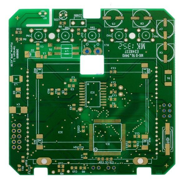
Led pcb manufacturing process is quite similar to a common pcb board development. A printed circuit board is a special plate where we apply conductive pattern. This pattern is comes with a dielectric, a material that has relatively poor current carrying capacity.
The most demanded today are two-layer printed circuit boards for electronics. Their main feature is that they contain a so-called conductive pattern on both sides at once.
The drawing on such devices is made of foil. The printed circuit board has special contact pads and mounting holes. This makes it easy to install the necessary components.
What is multilayer led pcb manufacturing process?
On double-layer or multi-layer boards, there are also special holes to provide an electrical connection between the layers. A special design helps in led pcb manufacturing process.
The modern world is hard to imagine without electronics. This cannot exist without high-quality printed circuit boards. This is why PCB fabrication is of such strategic importance to the world. In every country, enterprising people organize high-quality printing of boards. Hence, there is an opportunity for the development of electronics.
Varieties of modern printed circuit boards
There is a unified classification that is generally accepted for all states. According to her, printed circuit boards depend on the number of layers with a pattern:
- One-sided. Boards that have only one layer of a conductive element applied to one side of the dielectric.
- Double-sided. Models of boards that have two layers at once.
- Multilayer. This is a special type that is produced by layering several boards on top of each other. In such devices, the conductive element comes not only on one side, but also inside the board itself.
Pcb manufacturers use high quality dielectrics in led pcb manufacturing process. Today, most often, fiberglass is very common in production. It's worth noting that boards can also be both rigid and flexible.
Led Pcb Manufacturing Process
Modern printed circuit boards can be manufactured using one of two technologies - additive or subtractive. In the first case, a conductive pattern on the material forms using a chemical copper plating procedure.
In order for this process to be successful, a special protective mask comes to the dielectric. The peculiarity of the subtractive method is that a conductive pattern frms on an already foiled material by eliminating unnecessary areas.
The PCB manufacturing process consists of the following steps:
- Production of blanks for the board.
- Further processing of the workpiece.
- Installation of all necessary board elements.
- Conducting routine performance testing.
Today in many other European countries, there are a large number of private factories that specialize in led pcb manufacturing process. Almost each of these factories is able to carry out any of your projects to order. But this will require providing as much information as possible from a technical point of view.
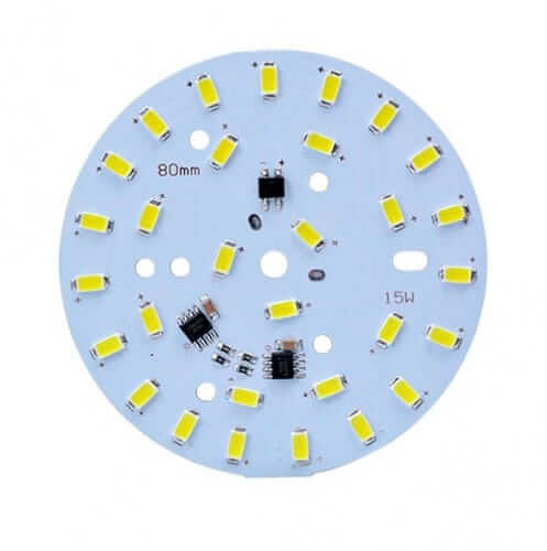
Installation of the necessary components on a printed circuit board
Soldering technology is very common to mount the elements on the board. This procedure allows you to get an absolutely permanent connection of parts by introducing molten metal.
For this, specialized equipment is popular to apply. However, we can perform the process itself at home, since it is not extremely difficult. However, the highest reliability and performance results can be possible only by ordering the manufacture of printed circuit boards. You can order it from specialized board manufacturing companies.
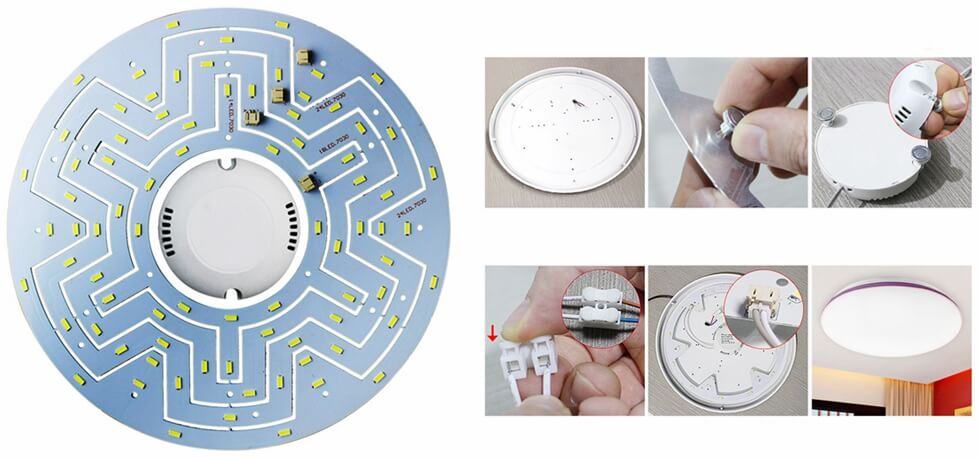
Many modern manufacturers with good reviews use a special protective mask to avoid short circuits during the soldering process. Also, the process of printing the boards includes the procedure for applying the marking. Moreover, it is necessary in order to facilitate the process of checking, assembling or repairing the board.
Led pcb manufacturing process stages
Every electronic printed circuit project developed has its own needs. PCBs have their own unique function for the project being developed. Therefore, manufacturing a PCB is a difficult and complex process that requires a lot of equipment and technology device. Moreover, it requires machinery investment to get a quality final product output consisting of exactly 13 steps. Let’s review led pcb manufacturing process steps:
1- PCB Design and Gerber File Obtaining
Pcb manufacturer makes drawing through PCB drawing programs and files are prepared in the format. The most common of these is the RS-274X Gerber format.
2- Pre-Production Engineering
PCB data (Gerber and Hole files) are used to generate production files. Production engineers compare the printed circuit board project's suitability for production against production standards..
3- Cutting FR4 Copper Plates Used in Production
For mass production, they go through multiplex procedure before production and paneled in a standard size. Paneled copper sheets appear via cutting. In addition, we should give importance to cleaning in this led pcb manufacturing process. Dirt or smudge can cause the circuit to short.
4- Plotter - Dry Film Printing
After checking the suitability of the card for production, we print the dry film of the card with a special printer. These printers use highly precise printing technology to present a detailed film of the design. Black ink shows the conductive areas of the PCB on the copper. Similarly, the remaining parts are insulating parts.
5 ETCHING Process (FR4 Abrasion of Copper Surface)
It is the removal of unwanted copper using a strong alkali solution. While etching finishes, PCB boards go into the acid pool for a certain period of time.
6- Soldermask Application
After drilling, the next step for led pcb manufacturing process is to cover the board with a solder mask, that is, protective paint. Furthermore, solder mask is to be in different colors. It generally uses green color. But depending on the condition of the printed circuit board project, it can be in red, blue, yellow, white and black colors. Moreover, you can ask according to customer preferences.
7- Led pcb manufacturing Surface Finish process
To ensure the solderability of the PCB board, the PCB boards go into the solder pool and removed. It is very important that the solderable area is smooth and flat.
Why Led Pcb boards?
Led pcb manufacturing process is a modern and indispensable circuit board manufacturing process. Electronics in human life has become completely irreplaceable, and electrical devices cannot exist without boards. Boards can be found both in cars and in military equipment, because their distribution is at the maximum at the moment.
The main purpose of printed circuit boards is to provide contact between interconnects. With the help of printed circuit boards, it is possible to reduce the overall dimensions of a device.
Conclusion
All modern electronics consists of led pcb devices. So it is especially important to control the quality of board production. That is why, it is important to know led pcb manufacturing process. Today, in many countries there are general standards and quality certificates. The production of printed circuit boards must necessarily comply with it.
PCB customization is one of the most popular services not only among large industrial facilities, but also among small businesses. If you urgently need manufacture printed circuit boards from scratch, then specialized stores and factories in China will help you with this.
