PCB Layer Stacking Capabilities
2022-11-18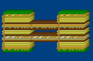
As circuit boards become more complex, bringing more functions and circuits together on a single board, compact PCB layouts need to provide more functionality. Therefore PCB is gradually moving to multi-layer PCB stack design, so what is PCB stack? And how do they work?
What is a PCB stack?
PCB stacking is a stack of copper and insulation layers that make up the PCB. In the most basic case, multi-layer PCB consists of at least three conductive layers. The bottom layer is synthesized with an insulating board, and each layer of the board is connected to the next.
Advantages of PCB stacking
- Improved functionality
Multi-layer PCBs can exponentially increase the speed and functionality of a device, resulting in a more powerful board
- Protection of internal layers
Layer stacking can help protect internal layers from external noise
- Reduces radiation
In high-speed layouts, PCB layer stacking can help you minimize radiation from your equipment. However, you need to be aware of impedance mismatches, which can lead to greater EMI emissions than with a normal PCB
- Reduce Cost
Good PCB stacking can help achieve low cost manufacturing by placing multiple circuits on a single board
How to create multilayer PCB stacks
Multi-layer PCB stacks should achieve the following minimum objectives through careful design to meet specific design requirements.
- Ground and power layers should be tightly coupled together
- Signal layers are adjacent to the plane
- High-speed signals are transmitted through the buried inner layer to control radiation
- Include multiple ground planes to reduce impedance and radiation
- Signal layers are coupled as close to their planes as possible
It is important to note that not every PCB stack can meet the above objectives; in fact, only an 8-layer board can meet all five objectives. You should work closely with your PCB engineering team to determine which goals are the highest priority for your PCB stack.
Common PCB layer stack types
There are five types of PCB layer stacks - 2-layer, 4-layer, 6-layer, 8-layer, and 10-layer. Exactly how many layers you need depends largely on the size of the circuit, the size of the board, and the board's EMC requirements. From there, you can determine the layout of the board.
2-Layer PCBs
Often referred to as a double-sided PCB, it is the most common type of PCB. A double-sided PCB consists of three material layers.
- Signal layer, which consists of copper and is approximately 0.0014-0.0021 inches thick
- Laminated core, separating the top and bottom copper layers, with vias to create connections between the two sides of the board.
- Bottom, second layer of copper similar to the signal layer, thickness of about 0.0014-0.0021 inches
4-layer PCB
In terms of PCB stacking, 4-layer PCB is the second most common choice for multilayer boards. However, the inner layers of a 4-layer PCB cannot be connected externally, so they are often used as power planes or for signal routing, which helps improve the quality of the alignment signal and reduces EMI emissions.
- Top Layer
- Prepreg
- Inner Layer 1
- Core board
- Inner Layer 2
- Prepreg
- Bottom layer
6-Layer PCB
6-layer PCB is functionally a 4-layer PCB with two additional signal layers
- Top layer
- Prepreg
- Grounding layer
- Core board
- Route layer
- Prepreg
- Route layer
- Core plate
- Power plane
- Prepreg
- Bottom layer
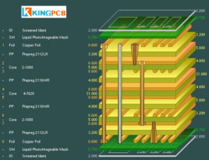
8-Layer PCBs
The 8-layer PCB stack offers more options than a 6-layer board by adding two layers for routing or performance. It is also the first board to market that achieves all five goals of a multilayer PCB design.
- Signal Layer 1
- Prepreg
- Grounding layer
- Core board
- Signal layer 2
- Prepreg
- Power plane
- Core board
- Grounding layer
- Prepreg
- Signal layer 3
- Core board
- Power plane
- Prepreg
- Signal layer 4
10-Layer PCB
If your design requires six wiring layers, then you should look at a 10-layer board.
- Signal layer 1
- Grounding layer
- Signal layer 2
- Signal layer 3
- Power plane
- Ground plane
- Signal layer 4
- Signal layer 5
- Power plane
- Signal Layer 6
KingPCB-Your source for quality multilayer PCBs
If you need to add functionality to your PCB, multilayer PCB lamination is a great option. No matter how many layers you need, KingPCB can help you.
KingPCB is located in Shenzhen, China and is one of the leading PCB manufacturers in China. Our high quality delivery and fast response makes us stand out from other suppliers. We also provide rigid-flex PCBs, flexible PCBs, HDI boards and other PCB related products.
Contact us now for a free inspection and quote for your multilayer PCBs.
