How to Avoid PCB Tombstoning Defects?
2022-10-17
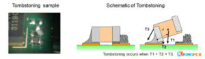
A tombstone defect is a kind of PCB failture. Tombstoning defects occur frequently and are caused by surface mount passive components that are partially lifted from the pads and erected to look like tombstones. But it is not as deadly as a burned component and can be 100% avoided.
What is a tombstone defect in PCB?
Tombstone defects are also called Manhattan effect, Stonehenge effect, or drawbridge effect. It occurs due to torque imbalance caused by different wetting humidity. Wetting is when the solder reaches a fluid state in order to attach the component leads to the pads. Ideally, the solder adheres to both pads while the wetting process is uniform, but unbalanced soldering can result in a standing monument.
Tombstone printed circuit boards are not limited to passive devices; it can also occur on SMT devices.
What are the causes of PCB tombstone defects?
- Unsuitable solder pad design
- Incorrect component placement
- Inconsistent pad size
- Nitrogen
- Uneven reflow oven temperature
- Chip placement parallel to reflow oven
- Inconsistent heating capacity of PCB material
How to avoid tombstone defects in PCBs?
Like other common PCB soldering defects, tombstone defects can be prevented. Please consider the following points.
PCB pad size
Always need to check the pad size is correct, too big or too small can lead to tombstone defects.
PCB surface treatment process
For small size components such as 0201 or 0402, avoid using traditional hot air solder leveling (HASL), which can lead to uneven surfaces.
PCB component placement
In the case of small components encountered, ensure that the alignment widths of the connection pads are equal and they should also be connected in a similar orientation.
Solder resist layer thickness
Ensure that the thickness of the solder resist layer is appropriate to prevent oxidation while not restricting the movement of the solder.
Inner copper overlay
Uneven copper coverage can lead to uneven heating.
Stencil design
A proper stencil design should ensure that there is sufficient solder paste, and in addition, there should be proper component overlap with the paste.
PCB testing
Each component needs to be tested to avoid affecting the function of the PCB. Common PCB tests are
-In-line testing
-Aging test
-Other functional tests
Trace wiring and power supply layer
The balance of PCB wiring is crucial.
To summarize
PCB soldering defects can lead to PCB failures, resulting in costly recalls and rework. To avoid possible PCB defects, it is important to choose an experienced PCB contract manufacturer. kingPCB provides one-stop PCB manufacturing services with professional wisdom, reliability testing and versatility.
If you have any questions, contact us now or by sales@kingpcb.com and we will respond immediately to any of your requests!
