Home PCB Fabrication-Quick turn High quality Low cost
2020-10-15Make Your Own PCB At Home
Looking for an easy home PCB fabrication guide? You're at the right place!
Making PCBs at home is not as complicated as it sounds. You can easily make one at home with a few supplies. In this article, we are sharing a simple step-by-step procedure to make PCBs at home. It's an interesting project to work upon, make sure you read it till the end!
WHAT IS PCB?
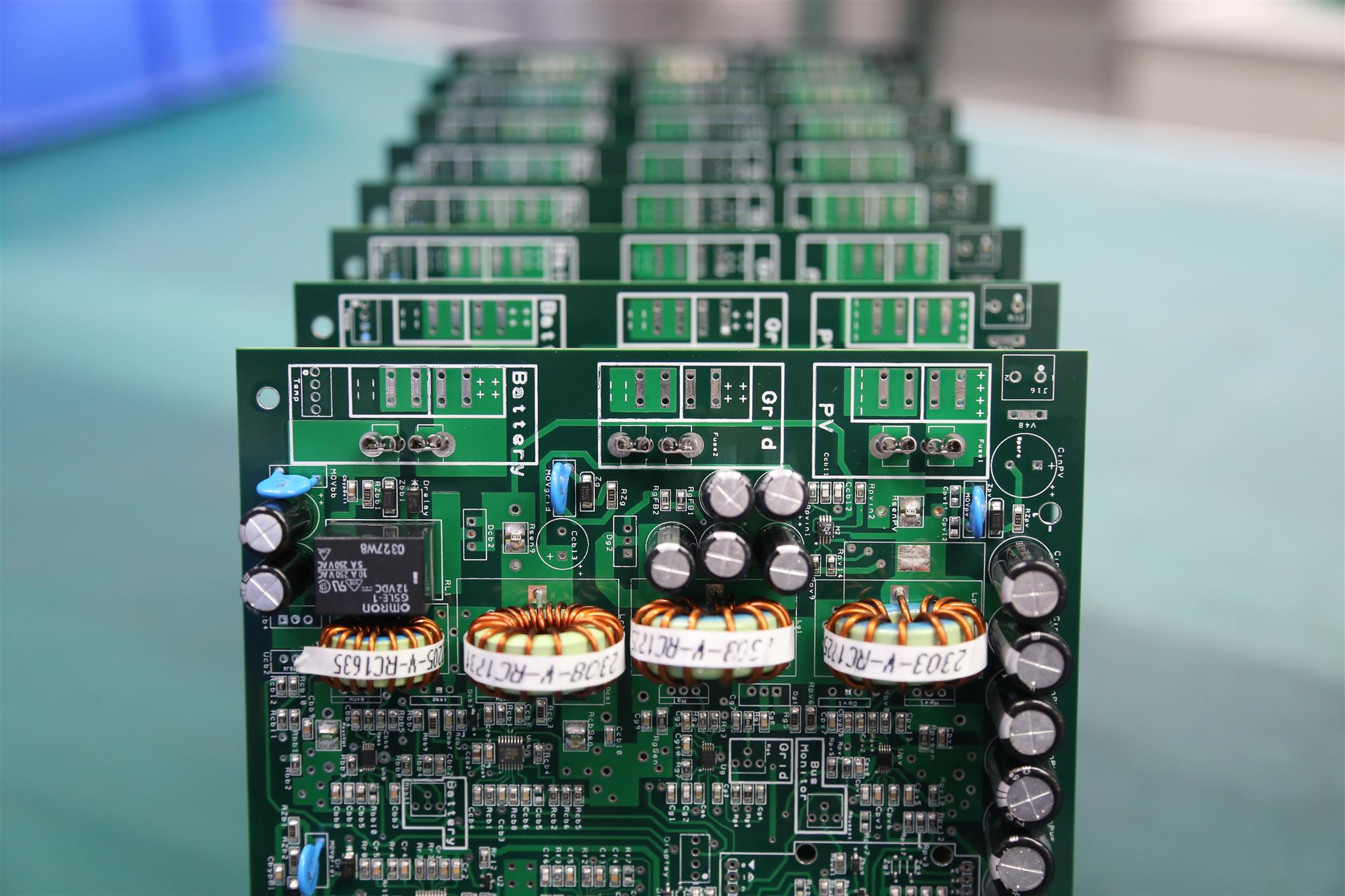
For those who don't know, PCB stands for Printed Circuit Board is used to support and connect the electronic components by using pads, conductive tracks and other functions crafted from a copper sheet fixed on to a non-conductive base.
A PCB has predefined conductive tracks on the copper sheet. These tracks eliminate the wiring and hence decrease the chances of faults arising due to poor connections. All you need to do is, simply solder the electric components by placing them on the PCB.
METHODS OF HOME PCB FABRICATION :
Generally, there are three main methods of fabricating a PCB. These are :
* Lamination Using Iron
* Handmade circuit on PCB
* Laser Cutting Method
Laser cutting is an industrial method and requires specialized tools that are not usually available at home. Hence, we will discuss the other two methods for making our DIY PCB.
1] CREATE A PCB CIRCUIT LAYOUT
The very first thing you need to do is to create a circuit layout for your PCB. Basically, you need to convert the schematic diagram of your circuit into a PCB layout. There are numerous PCB layout software to do this. You can use anyone to get a desired layout.
2] GATHER YOUR SUPPLIES
Next important step is to collect all the materials you'll be needing for this project. Here is what you'll need :
* Glossy paper or A4 size photo paper
* Photocopy machine or a printer
* Iron
* Etching solution
* Copper clad laminate
* Permanent marker (preferably black)
* Sandpaper
* Cotton
* Kitchen paper or tissues
* An old T-shirt
3] PRINT YOUR PCB LAYOUT ON THE GLOSSY OR PHOTO PAPER
Now, print your PCB layout design on the paper by keeping in mind the below tips :
* Print on the glossy side of the paper
* Set the printing ink color to black in printer and PCB layout software both.
* Print the mirror image
4] CUT THE COPPER PLATE
Take the copper plate and cut it according to the size of your layout.
5] SCRUB THE COPPER SHEET TO MAKE IT SMOOTH
Use a sandpaper or a steel wire ball to scrub the copper plate. This will smoothen its surface and also remove the photo resistant and oxide layer.
Sanding will also provide a better sticking surface.
6] PREPARE TO FABRICATE YOUR PCB
Now, the main part. Follow any one method to make your PCB.
Method 1: The Iron Method
You need to transfer the image from the glossy paper to the board by ironing it. For this, keep the top layer upside down. Place the copper sheet on printed design and make sure it is aligned properly with the layout. Tape the sides of the board to make sure it doesn't move from its place when you iron it.
Method 2: Making Handmade Circuit
If you're good at drawing, draw the circuit layout on the copper sheet using a pencil. Once you've perfected it, redraw using a permanent marker. Don't begin drawing the circuit with the marker because it will be impossible to erase it in case of any mistake.
7. Iron It On The Copper Plate
* Now, you need to print the layout on the copper plate by ironing. For this, heat your iron to the max temperature.
* Take the board and paper arrangement (you've done in the above steps) on a clean wooden table. Keep an old cloth by side and the photo paper should face you.
* Hold the paper by the cloth and put the hot iron on it from the other end for about 10 seconds. After that, iron it by applying some pressure for a good 10 to 12 minutes. Iron very slowly and firmly so that the design gets transferred properly
* Avoid touching the iron or the copper plate immediately after this step as it will be really hot at this time.
8. PEEL THE PAPER FROM COPPER PLATE
Place the copper plate into a bowl of slightly lukewarm water for 15 minutes. This will dissolve the paper and it will come off easily. After 15 minutes, slowly remove the paper.
If some of the traces get lighter, redraw them using black marker.
9. ETCHING
Be very careful while performing this step.
* First and most importantly, wear your rubber gloves and lay some newspapers on the surface so that the etching solution doesn’t spoil the floor.
* Fill a plastic container with water and add 2 to 3 teaspoons of etching solution to it.
* Place your PCB in this solution for about half an hour. This will remove the excess copper from the copper plate.
* After 30 minutes, take the PCB out using a plier and check if it is properly etched or not. If not, leave it again for 15 minutes.
* Keep stirring the solution with a wooden stick every 2 to 3 minutes till the plate is fully etched.
* Once done, take out the PCB and place it on a clean surface.
* Dispose of the etching solution very carefully. Note that it is very harmful for the animals and water organisms, so never throw it into any water source. Also, don't throw this solution into your sink, it may damage your pipes. Dilute it and then get rid of it.
12. APPLY THE FINISHING TOUCHES
Dip a cotton ball into thinner or nail polish remover and clean the copper plate using it. Now, wash it and dry it with a clean cloth or tissue paper. Give some final trimmings and you're done.
Now, simply drill a hole and solder your components.
CONCLUSION
There you have it! You own PCB at home using a few simple supplies. Glossy paper method is the best as it can print the PCB layout exactly. So, go for it instead of the handmade circuit technique.
