Copper-Filled Vias
2022-09-29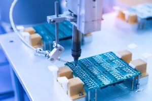
Vias are the conduits that carry signals between PCB layers, without which the printed circuit board would not function.
During the PCB manufacturing process, manufacturers add a layer of copper to the board substrate to conduct electricity and connect each PCB layer. Keeping the through-hole intact, copper plating is used to transmit the signal. To increase capacity, another conductive material can also be used to fill the plated vias.
Manufacturers will use epoxy resin and copper to fill the vias to make their PCBs more suitable for certain applications, although the additional material will also increase the cost of PCB production.
This article will describe the main uses of copper-filled vias and how they can enhance your PCB.
Copper-Filling process
When filling vias with copper, it is important to form a uniform layer of copper in the through-hole, too thin and too thick copper layer will not work. If improper techniques are used, too much copper may be produced resulting in increased PCB weight or too much copper on the copper traces. The result can lead to the inability to produce PCBs that meet specifications, defects and increased costs.
A common method for manufacturers to fill copper vias is to use pure copper to fill the vias, however, this method often results in voids that trap contaminants in the middle, which later in the heating process will break the connection between the PCB copper layers of the vias.
What are the benefits of copper-filled vias?
Compared to boards with only copper-plated vias, PCBs with copper-filled vias have the following advantages.
Increased thermal conductivity: In applications involving high temperatures, the high thermal conductivity of copper attracts this heat away from the critical areas of the PCB.
Increased conductivity: The conductivity of copper allows high currents to pass through deeper layers without overloading the PCB.
Application of filled vias and copper plated vias
PCBs with copper-filled vias increase capacity, but correspondingly increase production costs. When you decide on a PCB via, you have to consider the heat and voltage intensity that the application will generate. In low-stress applications, PCBs with plated vias can work properly without defects. High power, RF, microwave, and LED applications can use PCBs with copper-filled vias, and the currents used in high-power integrated circuits for this type of PCB are suitable for copper-filled vias.
Choose a trusted board manufacturer that can effectively coordinate the creation of PCBs with copper-filled vias or other special requirements. Contact us now to learn how we can meet your PCB needs.
