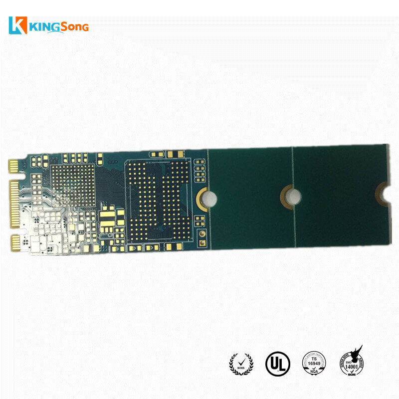
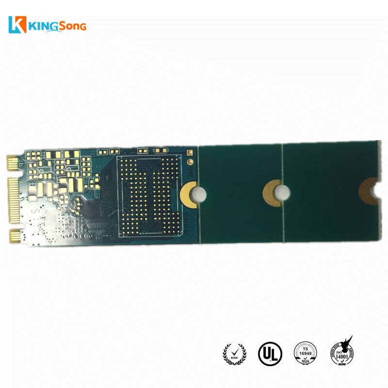

Multilayer PCB Board Manufacturer Service For SSD Product
Layer: 4
Base Material: FR4
Copper Thickness: 1oz
Board Thickness: 1.6mm
Surface Finishing: Immersion Gold
Min. Order Quantity: NO
Supply Ability: 30~50 thousand ㎡/Month
Service: EMS/OEM/ODM
Payment Terms: T/T, Paypal, WU, etc.
Port: Shenzhen
With more than 10 years of PCB manufacturing experience, KingSong provides high-reliability products and provides our customers with high-value, high-quality, and guaranteed quality production services.
Multilayer PCB is the printed circuit board with more than two layers, such as 4 layers, 6 layers, 8 layers, 10 layers, etc. It is double-sided multiple. And with common features as more than two layers conductive traces, separated by insulating material between the layers, and the layer between the conductive traces must be connected through drilling, lamination as required. Multilayer PCB board is with multi-layer conductive wire, high-density drilling. It is widely used in electronic equipment.
Multi-layer PCB board and Double Sided PCB board are the main circuits KingSong PCB Manufacturer provides. Kingston could support customer multilayer PCB production up to 38 layers by prototype and middle run. Multilayer printed circuit board is more and more used by different PCB designers due to the multi-layer PCB board could meet the requirement of overload of weight and volume.
| Item | Mass Production | Prototype |
| Layers | 1-8 Layers | 1-36 Layers |
| Max. Panel Size | 600*770mm (23.62″*30.31″) | 600*770mm (23.62″*30.31″) 500*1200mm (19.69″*47.24″) |
| Max.Board Thickness | 8.5mm | 8.5mm |
| Min. Board Thickness | 2L:0.3mm, 4L:0.4mm, 6L:0.8mm |
2L:0.2mm, 4L:0.4mm. 6L:0.6mm |
| Min Inner Layer Clearance | 0.1mm(4mil) | 0.1mm(4mil) |
| Min Line width | 0.075mm(3/3 mil) | 0.075mm(3/3 mil) |
| Min Line space | 0.075mm(3/3 mil) | 0.075mm(3/3 mil) |
| Min.Hole Size | 0.15mm(6mil) | 0.15mm(6mil) |
| Min plated hole thickness | 20um(0.8mil) | 20um(0.8mil) |
| Min Blind/Buried hole size | 0.1mm(4mil) | 0.1mm(1-8layers)(4mil) |
| PTH Dia. Tolerance | ±0.076mm(±3mil) | ±0.076mm(±3mil) |
| Non PTH Dia. Tolerance | ±0.05mm(±2mil) | ±0.05mm(±2mil) |
| Hole Position Deviation | ±0.05mm(±2mil) | ±0.05mm(±2mil) |
| Heavy Coppe | 4oz/140μm | 6oz/175μm |
| Min S/M Pitch | 0.1mm (4mil) | 0.1mm (4mil) |
| Soldermask colour | Green, black, Blue, White, Yellow, Red | Green, black, Blue, White, Yellow, Red |
| Silkscreen colour | White, Yellow, Red, Black | White, Yellow, Red, Black |
| Outline | Routing, V-Groove, Beveling punch | Routing, V-Groove, Beveling punch |
| Outline Tolerance | ±0.15mm ±6mil | ±0.15mm (±6mil) |
| Peelable mask | Top, bottom, double sided | Top, bottom, double sided |
| Controlled Impedance | +/- 10% | +/- 7% |
| Insulation Resistance | 1×10¹²Ω(Normal) | 1×10¹²Ω(Normal) |
| Through Hole Resistance | <300Ω(Normal) | <300Ω(Normal) |
| Thermal Shock | 3×10sec@288℃ | 3×10sec@288℃ |
| Warp and Twist | ≤0.7% | ≤0.7% |
| Electric Strength | >1.3KV/mm | >1.4KV/mm |
| Peel Strength | 1.4N/mm | 1.4N/mm |
| Solder Mask Abrasion | >6H | >6H |
| Flammability | 94V-0 | 94V-0 |
| Test Voltage | 50-330V | 50-330V |
PCB lead time: (if you need urgent service,we also can meet)
| Description | Double Layer | 4 Layer | 6 Layer | 8 Layer | 10 Layer or above |
| Sample(WD) | 3-5 | 7 | 8 | 10 | 12 |
| Mass production(WD) | 7-9 | 10-12 | 13-15 | 16 | 20 |
Package:
The inner vacuum packing, Outer standard carton box packing.
Shipping:
1. By DHL,UPS,FedEx,TNT etc.
2. By sea for mass quantity according to the customer’s requirement.
If you need a quotation for your PCB projects, please provide the following info:
1. Quote, quantity.
2. Gerber file in a 274-x format.
3. Technical requirement or parameters (material, layer, copper thickness, board thickness, surface finishing, solder mask/silkscreen color…).

Don't know enough?
Welcome to contact us And Start Your Business Now!


Shentengyao Building, Fuhai, Shenzhen 518103 China
