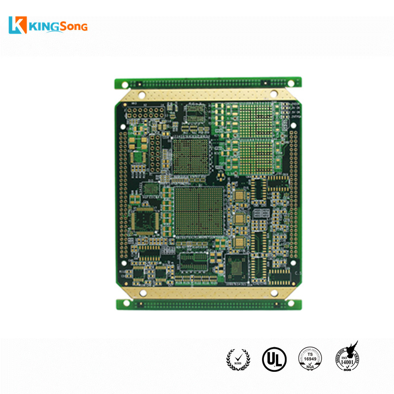
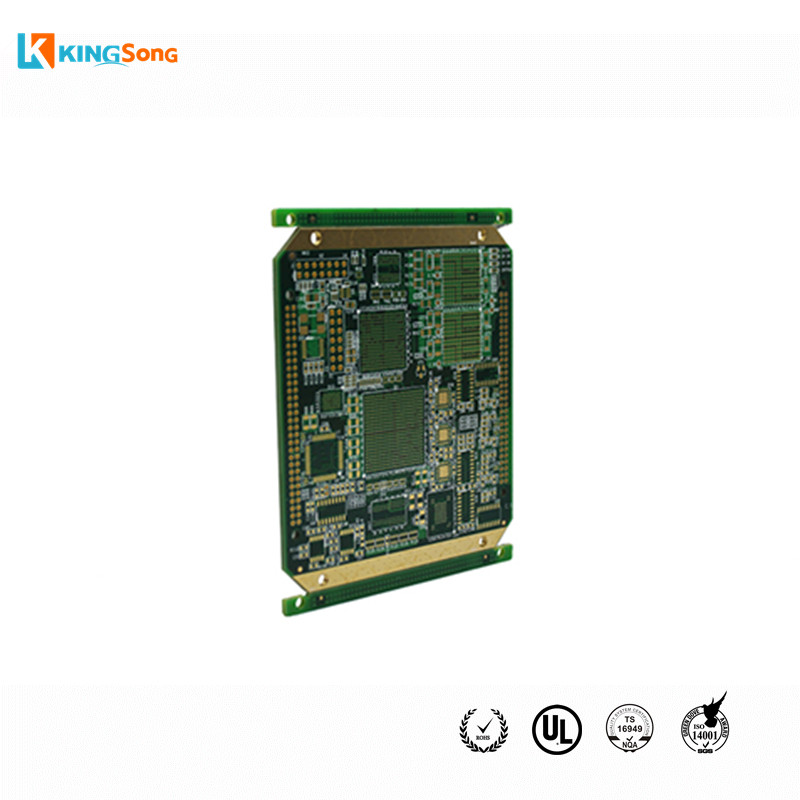
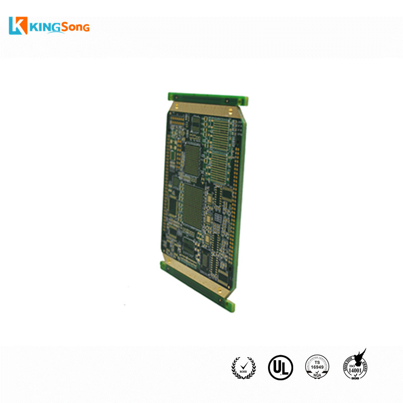

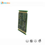
16 Layers High TG Gold Plated PCB Circuit Boards
Layer: 16
Base Material: High Tg FR4
Copper Thickness: 1oz
Board Thickness: 2.43mm
Test Way: 100% E-Test
Min. Order Quantity: NO
Supply Ability: 30~50thousand ㎡/Month
Service: EMS/OEM/ODM
Payment Terms: T/T, Paypal, WU, etc.
Port: Shenzhen
With more than 10 years of PCB manufacturing experience, KingSong provides high-reliability products and provides our customers with high-value, high-quality, and guaranteed quality production services.
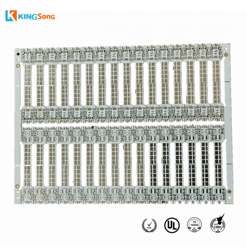
This Printed Circuit Board is a 16 Layers High Tg Gold Plated PCB Circuit Boards, used in Industrial Control, some like Core board, A PCB Circuit Board with Immersion Gold Surface Finishing is a coating between a component and a bare PCB circuit board, KingSong Technology as a professional PCB Manufacturer are not only offer High Tg PCB board, but also Immersion Gold PCB, 16 layer PCB or more Multilayer PCB, etc.
| Item | Mass Production | Prototype |
| Layers | 1-8 Layers | 1-36 Layers |
| Max. Panel Size | 600*770mm (23.62″*30.31″) | 600*770mm (23.62″*30.31″) 500*1200mm (19.69″*47.24″) |
| Max.Board Thickness | 8.5mm | 8.5mm |
| Min. Board Thickness | 2L:0.3mm, 4L:0.4mm, 6L:0.8mm |
2L:0.2mm, 4L:0.4mm. 6L:0.6mm |
| Min Inner Layer Clearance | 0.1mm(4mil) | 0.1mm(4mil) |
| Min Line width | 0.075mm(3/3 mil) | 0.075mm(3/3 mil) |
| Min Line space | 0.075mm(3/3 mil) | 0.075mm(3/3 mil) |
| Min.Hole Size | 0.15mm(6mil) | 0.15mm(6mil) |
| Min plated hole thickness | 20um(0.8mil) | 20um(0.8mil) |
| Min Blind/Buried hole size | 0.1mm(4mil) | 0.1mm(1-8layers)(4mil) |
| PTH Dia. Tolerance | ±0.076mm(±3mil) | ±0.076mm(±3mil) |
| Non PTH Dia. Tolerance | ±0.05mm(±2mil) | ±0.05mm(±2mil) |
| Hole Position Deviation | ±0.05mm(±2mil) | ±0.05mm(±2mil) |
| Heavy Coppe | 4oz/140μm | 6oz/175μm |
| Min S/M Pitch | 0.1mm (4mil) | 0.1mm (4mil) |
| Soldermask colour | Green, black, Blue, White, Yellow, Red | Green, black, Blue, White, Yellow, Red |
| Silkscreen colour | White, Yellow, Red, Black | White, Yellow, Red, Black |
| Outline | Routing, V-Groove, Beveling punch | Routing, V-Groove, Beveling punch |
| Outline Tolerance | ±0.15mm ±6mil | ±0.15mm (±6mil) |
| Peelable mask | Top, bottom, double sided | Top, bottom, double sided |
| Controlled Impedance | +/- 10% | +/- 7% |
| Insulation Resistance | 1×10¹²Ω(Normal) | 1×10¹²Ω(Normal) |
| Through Hole Resistance | <300Ω(Normal) | <300Ω(Normal) |
| Thermal Shock | 3×10sec@288℃ | 3×10sec@288℃ |
| Warp and Twist | ≤0.7% | ≤0.7% |
| Electric Strength | >1.3KV/mm | >1.4KV/mm |
| Peel Strength | 1.4N/mm | 1.4N/mm |
| Solder Mask Abrasion | >6H | >6H |
| Flammability | 94V-0 | 94V-0 |
| Test Voltage | 50-330V | 50-330V |
PCB lead time: (if you need urgent service, we also can meet)
| Description | Double Layer | 4 Layer | 6 Layer | 8 Layer | 10 Layer or above |
| Sample(WD) | 3-5 | 7 | 8 | 10 | 12 |
| Mass production(WD) | 7-9 | 10-12 | 13-15 | 16 | 20 |
Package:
The inner vacuum packing, Outer standard carton box packing.
Shipping:
1. By DHL, UPS, FedEx, TNT, etc.
2. By sea for mass quantity according to customer’s requirement.
If you need a quotation for your PCB projects, please provide the following info:
1. Quote, quantity.
2. Gerber file in a 274-x format.
3. Technical requirement or parameters (material, layer, copper thickness, board thickness, surface finishing, solder mask/silkscreen color…).

Don't know enough?
Welcome to contact us And Start Your Business Now!


Shentengyao Building, Fuhai, Shenzhen 518103 China
