Vias in BGA Pads
2022-11-22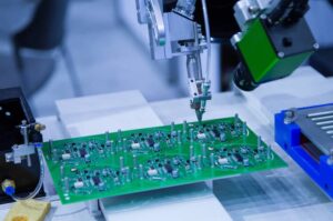
Have you ever considered using Via-in-pad when designing your PCB?
Via-in-pad designs are becoming increasingly popular, and if you are unsure whether to use a printed circuit board with traditional vias or vias in pads. This article will take you through what vias in pads are.
What is a Vias-in-pads?
This is an in-pad vias design, which is simply a via under the pad.
The vias in the tray is mainly used for BGA packaging area, because its surface needs to be soldered or chip paste. The requirements for its accuracy and acceptable area are high, as is the surface flatness to prevent false soldering or bad nodes due to uneven chip placement.
Advantages of the vias-in-pads
VIA-IN-PAD, also known as VIP design, the main advantage is that it reduces the area required for vias, making it easier to manufacture miniaturized PCBs and significantly reducing the board area required for signal routing.
By connecting the vias directly to the layer below the component, you can route signals without going outside the device package.
Traditional Through-Hole vs. vias-in-pads
In a traditional PCB via layout, you can use a solder resist layer to prevent solder from entering the via and avoid electrical connection problems.
When you use vias-in-pad, the practice of using traditional via will not work and the via-in-pad must completely fill the via so that there is no air trapping and degassing.
Typically, PCB manufacturers fill the through-holes in the pads with epoxy after they have been mechanically drilled and plated. Or, you can laser ablate your vias and fill them with copper. What you choose to do will depend on your specific application and the needs of the printed circuit board and the size of the vias. The main issue that determines the process is the pad diameter.
Choosing traditional vias or vias-in-pads?
With the development of lighter, thinner and smaller electronic products, PCBs are pushing towards higher density and more difficult development, so the size of the components is getting smaller and smaller. With small pin spacing, it is difficult to wire the pins inside the package, so it is necessary to change the layer of hole punching wiring.
In the case of sufficient spacing, it is suggest that not use the vias-in-pads design, because the manufacturing of vias-in-pads high cost, production cycle time is also longer.
Explore KingPCB's PCB over-hole manufacturing technology
KingPCB has extensive experience in printed circuit boards, whether it is blind vias, micro vias, or plate vias, we can provide you with high quality services.
Contact us now for more information about our PCB manufacturing!
