Everything You Need To Know About A Printed Wiring Assembly
2020-09-21Everything You Need To Know About A Printed Wiring Assembly
A printed circuit board (PCB) is simply a board which electrically connects components using pads, conductive tapes and other components eatched from a copper foil and laminated on a non-conductive substrate. They can be single sided with one layer of copper or double sided with two layers and even multi-layered. A printed wiring assembly is the board made after all the electronic parts and components have been installed and soldered on the PCB and is now ready to perform the function for which it was designed. In rigid assemblies, the PCB makes use of a solid base to prevent it from twisting. On the contrary, flexible PCBs allow twisting and bending according to our requirements.
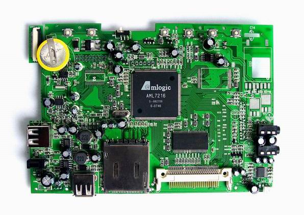
This printed wiring assembly is designed to offer a central hub to integrate all the electronic components within a device. By using multiple layers for creating the PCB, there are conductive tracts or pathways laminated on a substrate material. These tracks are utilised to conduct electricity which acts as a circuit to all the components which are soldered on the board. This powers the device while providing safe transmission and insulation of electric current. A printed wiring assembly is often confused with the term PCB. However, a PCB becomes a printed wiring assembly after the soldering, testing and feedback processes.
ADVANTAGES:
There are several myriad advantages of a printed wiring assembly over the traditional circuit boards making it the go-to solution to all electronics manufacturers. Some of the benefits are listed below:
1. Saves time and space through eliminating bulky components and wires and their connection cables.
2. Remains rigid regardless any movement of the circuit board.
3. Eliminates short circuits and loose connections through copper tracks instead of connected components.
4. Increased scalability of the printed wiring assembly allows for their use in a wide range of applications inclusive of large production runs.
5. The use of shorter pathways decreases the noise level leading to low pickup of electromagnetic waves and radiation.
6. A printed wiring assembly is often produced at low costs. Produced more rapidly because they are efficiently and easily produced in masses.
7. These can be counted upon for reliable operations. The copper tracks helps connect everything smoothly and without any loosening.
COMPONENTS:
The printed wiring assembly board has a number of vital hardware components which plays its role in powering the device. The components include:
1. Diode: Diode is a component used to streamline the electricity through a single direction and block the others.
2. Capacitors: These are designed for holding an electrical charge for operating the device.
3. Resistors: Resistors are color-coded controls which allows the electric current to flow through.
4. LED: It is a light-emitting diode that lights up whenever an electric current flows through it.
5. Switches: Another vital hardware part of a printed wiring assembly are the switches. It prevents or allows the current from flowing, depending on whether those are open or closed switches.
6. Inductors: It acts as a passive component to resist a sudden change in the current.
7. Battery: The battery links voltage to the board.
PROCESS:
There are a number of individual stages for the printed wiring assembly process. It is essential that all these stages are well-integrated for it to come together properly. Each and every step should be compatible with the further step. Also for maintaining high quality, the output to input feedback must be considered at every stage. In this way, all problems are quickly detected and the necessary changes can be made from time to time.
1. Solder paste: Before adding the components to the board, solder paste is added to all those areas where it is required. Typically, the areas that require solder are the component pads. A solder screen helps achieve the same. The solder paste is made up of flux mixed with tiny grains of solder. Using the screen which is placed directly on the board alongside registering it in the correct place, a runner is moved all over the screen to squeeze a small amount of the paste in the screen through the holes and on the board. The amount of solder paste deposited should be controlled to ensure the joints contain the right amount of it.
2. Pick and place: Prior to applying the solder paste to the PCB, the printed wiring assembly process is moved ahead to the pick and place stage. The surface mount components are placed on the prepared PCB. These components are soldered on the board's surface in this next step. Traditionally, this process was manual and assemblers had to manually pick and place the components with a pair of tweezers. Nowadays, the manufacturers have automated the process. The components are all automatically placed on top of the solder paste by the machine in preprogrammed locations.
3. Reflow Soldering: At this stage, the solder paste has to be solidified. In short, the solder paste and the components on the board all need to remain in place. The printed wiring assembly accomplishes this through "reflow". After the conclusion of the pick and place steps, the board is shifted to a conveyor belt. This belt is moved through a huge reflow oven similar to a commercial pizza oven. This kind of oven is comprised of a series of heaters which heats the board gradually to a temperature of about 480 degrees Fahrenheit or 250 degrees Celsius. This melts the solder in the paste. The cool heaters then lets the melted solder to cool down and solidify in the controlled manner.
4. Inspection and Test: After the soldering process, an automatic optical inspection is carried on the printed wiring assembly to detect misplaced components, poor joints or even wrong. There is a thorough test done for use before letting it out.
CONCLUSION:
A printed wiring assembly is a circuit board after all placement, soldering and inspection processes are performed on a PCB. The common applications of the assembly include computers, printers, stereos and television, digital clocks, mobile devices and musical instruments. They support a wide range of technology and products in almost every conceivable industry. One needs to always check for the prototype development, design and layout, quality and the manufacturing integration while purchasing from a vendor.
