PCB Manufacturer: A Step by Step Guide
2019-10-06PCB Manufacturer: Excellent Guide on Printed Circuit Boards
PCB is being a fundamental part of all the computational electronics and it requires to indebt analysis, yet, PCB Manufacturer simply assumes that everyone is familiar with this key concept. Thus, they do not shed light on its effectiveness and importance.
To ensure that you make the right possible decision when it comes to choosing an excellent, yet cheap Chinese PCB Manufacturer, you need to have complete knowledge regarding what a PCB is and its basics. Once you are familiar with the basics, you will be able to make a more knowledgeable decision for the better of your business.
In the course of this article, we will provide you a complete systematic guide on the Printed Circuit Boards. The breakdown of the guide is as follows
- What is PCB?
- Composition of PCB
- Common Terminologies
What is PCB - PCB Manufacturer?
Printed Circuit board, or even called Printed Wiring Cards or Printed Wiring boards are an imperative part of all computational electronics. Initially, the process of point-to-point wiring came into play in order to create circuits. However, the laborious process often led to short circuits and wire junctions due to wire aging and cracking.
To make these circuits robust, the designers came up with a significantly advanced concept, wire wrapping. The idea was to wrap the small gauge wire around a post at each connection point. This resulted in the creation of a gas-tight connection. The connection turned out to be extremely durable and efficiently altered.
Initially, the PCBs were expensive. However, the transition of electronics from vacuum tubes to integrated circuits and silicon circuits reduced the overall cost. In addition, to the cost, the size of the electronics decreased significantly. Electronics started to become an important part of consumer good, pressuring the manufacturers to look for effective, cost-efficient and reliable alternatives, thus the PCB was born.
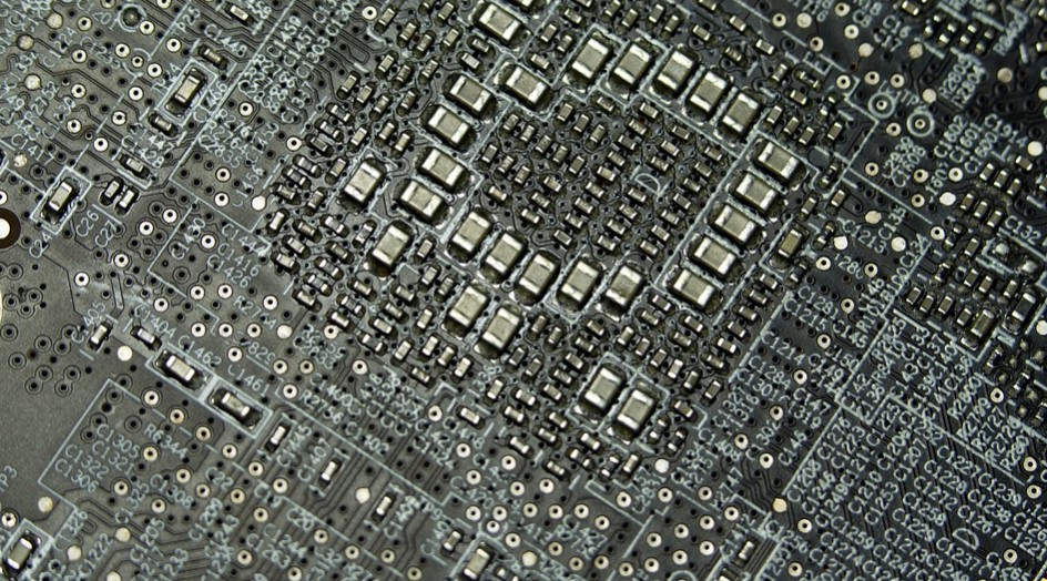
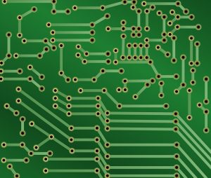
PCB is a board that has pads, and lines interacted at several points. Various connectors and components electrically connect to each other. With PCB, it is possible to rout signals and power between physical devices. The metal that allows the electrical connection between the electronic components and the surface of the PCB is Solder.
In addition, to form a strong and reliable connection between the device and PCB, the Solder is also a strong mechanical adhesive.
Composition of PCB - PCB Manufacturer
Different PCB manufacturers use different composition for the boards. Understanding the composition of PCBs might be a little complicated, as there are layers of different materials that are laminated together using adhesive and heat. These layers and their interconnection form a single object, PCB.
However, you do not have to worry, as we will provide you with complete information on the structure of PCB while keeping the complexity level minimal.
So, let us get to it.
Read More:What is the meaning of Multi-layer in PCB Board?
FR4
For years, Fiberglass, especially FR4, has been the common designator for the base material. Mainly because PCB requires a robust substrate and fiberglass act as a solid core. It provides the circuit the thickness and rigidity they require in order to function seamlessly.
The evolution of technology did lead to other flexible materials to act as the base material for PCB. PCBs are built on high temperatures and flexible plastics such as Kapton. Manufacturers tend to use Kapton or other equivalent materials for building strong and long-lasting printed circuit boards.
Since a PCB consists of several layers including epoxy prepreg, di-electric cores, and copper, thus it comes in various sizes and thicknesses. Several Printed Circuit Boards achieve their thickness due to several prepreg sheets and numerous core thickness sheets.
The customers have the option to choose between different laminate thickness including 2.3mm, 2.0mm, 1.5mm, 1.2mm, 1.0mm, 0.8mm, 0.6mm, 0.5mm, 0.4 mm, and 0.2mm among others. In order to achieve an extremely thin board, the manufacturer’s limit themselves to using only one layer of the core, and two copper layers.
In order to incorporate more copper, they will have to use more core and prepreg layers, thus increasing the thickness of the circuit in the end. For a board to be mechanically sound, the layers should be evenly distributed i.e. an odd number of dielectric layers and an even number of copper layers. When boards use thinner copper options, they are able to achieve a high number of layers without adding a lot to their thickness aspect.
The quality of the boards has a direct impact on its overall cost. Using copper or glass fiber will increase the cost; however, it will offer durability at the same time. In case, you choose to look for a cheap alternative such as phenolics or epoxies, you will not get durability.
Usually, a cheap alternative is easy to identify, as it has a strong smell. You might find the smell similar to that of low-end consumer electronics, as the same substrates are present in those electronics. However, there are PCB Manufacturers, especially some Chinese PCB manufacturers, such as KingSong PCB Technology Ltd, that offer robust Printed Circuits boards at a minimal price.
Copper
A thin copper layer comes next. To laminate the thin copper foils to the board, PCB Manufacturers, use heat and adhesive. Usually, a double-sided PCB contains copper on both sides. To reduce the price some manufacturers might limit the use of copper foil to only one side.
By double-sided PCB, we mean it contains two copper layers. A PCB can even have one layer or up to 16 layers. It all depends on the quality, the cost, and the requirement of the circuit. Copper thickness is specified by weight and it can vary.
Usually, the PCB developers use ounces per square foot. Most PCB Manufacturer comes with one ounce of copper per square foot. In case, the circuits are to handle high power, they might incorporate two to three ounces of copper per square foot. Every ounce translates to about 1.4 thousandths of an inch in terms of copper thickness.
Soldermask
Soldermask layer comes on top of the copper foil. It is basically the layer that ads color to the Print Circuit boards. It usually gives them a green color, however, in some cases, you may find it to be of a different color.
To prevent other metals to be exposed to copper traces, the manufacturers overlay a Solder layer on top of the copper layer. This step insulates the copper layer and it helps prevent solder jumpers as well as aid the users to solder in all the right places.
If you look at the circuit picture, you will notice that the entire circuit is covered in green expect the SMD pads and the silver rings. This allows easy and injury less soldering of the SMD pads.
Silkscreen
To add the symbols, number, and letters to PCB, Chinese PCB Manufacturers add a while silkscreen layer on top of the solder mask layer. The reason for adding numbers and indicators is to enhance the human understanding of the board. For instance, a manufacturer might use a label to indicate the function of every pin or an LED on the board.
In general, manufacturers, even cheap Chinese PCB manufacturers tend to use white Silkscreen. However, there are other options available for instance, yellow, red, gray or black. To retain uniformity, it is uncommon to use more than one color on a single board, but there is no hard and fast rule of not using more than one color.
Terminology
Now that you have an idea of what is a PCB, let’s focus on some of its common terminologies. These terminologies will help you deal with affordable and cheap Chinese PCB Manufacturer in an effective manner.
Annular Ring: The ring is of copper and it is installed via a hole in the circuit board.
DRC: DRC or formally known as the Design Rule Check ensures that the PCB design is error-free. It allows the manufacturer to find problems such as small drilled holes, skinny traces or traces that might get touched incorrectly.
Drill Hit: The actual place of the drill-hole on the board. The design specifies the place; however, drill hits are among the most common manufacturing defects.
Finger: To create a connection between two circuit boards, these boards come with exposed metal pads located along their edges. For example, the cartridge-based video games, or memory boards, etc.
Mouse bites: To create a weak spot in the board so that it is possible to break it after the face, the manufacturer clusters a number of drill heads close together. It is basically an alternate to v-score for separating boards from the panels.
Pad: It is the exposed metal on the surface of the board. All the soldering is conducted via these pads.
Panel: Small boards are put together to create a big circuit board. These small boards can easily be separated from the large board before the use. It is difficult for the automated circuit board to handle several smaller boards, however, incorporating these boards into one big board, increases the speed significantly.
Paste Stencil: It permits the deposition of solder paste in specific areas during the assembly. It is a thin, metal or in some cases plastic stencil lying over the board.
Pick and Place: The processor the machine that a PCB Manufacturer chooses in order to place the components on the board.
Plane: Better known as Pour, it is a continuous block of copper on the circuit board. Instead of having a path, it has defined borders.
Plated Through Hole: The hole is plated through the board and it has an annular ring. It might act as a connection point.
Pogo Pin: Spring-loaded contact, to make a temporary connection for programming and testing reason.
Reflow: Creating joints between components leads and pads via melting the Solder.
Silkscreen: The numbers, letters or symbols present on the circuit board. Mostly, they come in one color and low resolution.
Slot: Slots are the holes on the circuit board that are not round. Some slots are plated, whereas others are not. Slots increase the cost of the board, as they require extra cutout time.
Solder Paste: The PCB Manufacturer uses paste stencil along with solder suspended in a gel medium to apply onto the surface mount pads. The layer comes before the placement of the PCB component. When the solder in the paste melts, it creates electrical and mechanical joints between the components and the pads.
Solder Pot: A pot containing a small amount of molten solder, and it often hands solder boards with through-hole components. The manufacturer dips the board into the molten solder. However, they leave all solder joints on all exposed pads.
Soldermask: In order to prevent corrosion, short circuits, or similar problems, the manufacturer place layer of protective material onto the board. Usually, the layer is of green color; however, you do find other colors as well. Solder leaves that pads that are to be solder to, but it covers up all the signal traces.
Solder Jumper: Solder jump acts as a medium to connect either two pads or two pins adjacent to each other. It is a small, blob of solder. The manufacturer needs to be extremely careful with it, as it can lead to unwanted shorts.
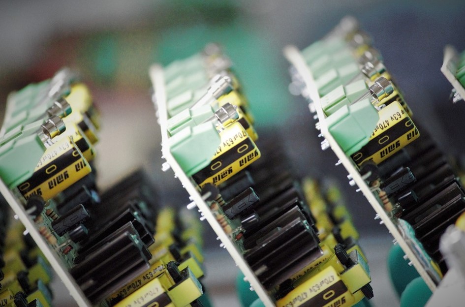
Surface mount: An effective and modern method of populating the boards, allows components to, effectively sit on the board without paying heed to the leads passing through the holes.
Thermal: It a small surface that connects a plane to a pad. In case, the pad is not able to relieve thermally, getting the pad to a high enough temperature can be troublesome. This will lead to problems while creating a good solder joint. It is easy to identify an improperly thermally relieved pad. The pad will feel sticky, and it will take a lot of time in order to reflow.
Thieving: Dots, gridlines, or hatching of copper present in the areas of the board where no traces or plane exists. It decreases the complexity level of etching as minimal time is consumed to remove the unnecessary copper.
Trace: The copper continuous path on a Printed Circuit Board.
V-Score: It is a part of the board, and it allows easy separation of the board along a line.
Via: It is a hole in the PCB board that passes a signal from layer to layer. To ensure that tented vias are not soldered, they are covered with a solder mask. However, the manufacturer uses untented vias in places where the components and the connectors might form a link.
Summary
Printed Circuit Board is an imperative part of the electronics; therefore, it needs to be of high quality. Basic understanding of PCB along with the knowledge of their common terminologies will help you choose the best and the most reliable PCB Manufacturer.
Of course, there are several PCB Manufacturers, out there, but not all are worth your time and money. Many of these manufacturers may claim to be the most affording manufacturer; however, they will not be able to maintain quality.
Limited manufacturers, such as KingPCB are able to retain quality while keeping their prices competitive. KingPCB is among the leading, yet extremely affordable and cheap Chinese PCB Manufacturer. Their years of experience in the PCB production allow them to design and develop top-class Printed Circuit boards.
Their knowledgeable staff has an indebt knowledge regarding every aspect of the Print Circuit Board manufacturing. They will use high-quality material for the core base to increase robustness. The will incorporate copper foil to decrease thickness while adding more layers to the board.
They always ensure that every hole is properly plated and components can be smoldered seamlessly. The quality of their Printed Circuit Boards is the best that you can find on the market. Their competitive price is their biggest competitive edge. So, be sure to check out their official website in order to learn more about them. Read more about SMT PCB.
