Knowing the Best Digital PCB Assembly and Designing Process
2020-05-25The Best Digital PCB Assembly and Designing Process
Electronics are a vital part of our day to day lives. Everything from the smartphones to cars are available with electronic components. The Printed electric board can be said as the heart of all electronic components, which is also known commonly as the digital PCB.
A lot of people are immediately able to recognize printed circuit boards just by seeing these. These are green chips that get covered in copper parts and lines that you’ll find at heart of gutted electronic devices. These are made through copper lines, Fiberglass along with other parts of metal, all these boards remain held together with epoxy and are insulated through soldering mask. The solder mask would be where the characteristic green color would be available from.
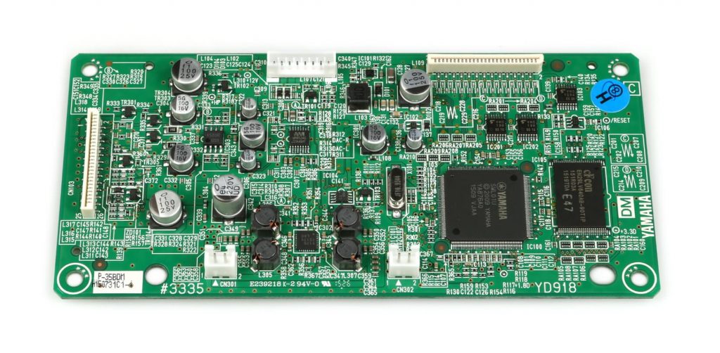
However, did you ever observe the boards with the components stuck solidly on? These can never be regarded as only PCB board decorations. Advanced circuit boards are not able to provide functionality until components become mounted on it. PCB with the components mounted on is known as assembled PCB and the process of manufacture is known as the digital PCB assembly or in short PCBA.
The copper lines on the bare board are known as traces, the electrically linked components and connectors to each other. They run the signals between all such features, letting circuit board for functioning specifically in a designed way. Such functions mainly range from simple to complex, yet PCB size remains smaller compared to thumbnail.
How such devices are made?
The digital PCB assembly process is quite simple, and consists of various manual and automated steps. In each step of the process, the board manufacturer can select from both the digital automated and manual options and the one for selecting. For helping in better understanding of digital PCB assembly process from the start to finish. Thus, each step can be explained below.
The basics of PCB design
PBCA process begins mostly with basic PCB unit: base, consisting of various layers, with each one playing significant role in final PCB functionality. All such alternating layers have:
Copper: Thing conductive copper foil gets added for each of the functional PCB side – on one side if this remains a single-sided PCB, and on both sides if the PCB is double sided. The layer is of the copper traces.
Soldering mask: On copper layer top there is solder mask, providing each PCB with the characteristic green color. This insulates traces of copper from unintentionally contacting various other conductive materials, that results in a short. To simply state, the solder is meant for keeping everything in place. Solder mask holes are present where solder gets applied for attaching all board components.
This is an essential step to smoothly manufacture the PCBA as it can stop soldering from taking place on the unwanted parts with the avoided shorts.
The Silkscreen: White silkscreen is final layer present on PCB board. The layer is vital for adding labels in PCB in form of symbols and characters. This is ideal for indication of each component’s function on board.
The materials and components largely remain identical across all of the PCBs, with substrate being the exception. The PCB substrate material keeps changing accordingly with certain qualities – like bendability and cost – each designer looks for in the newest finished product.
Three of primary types of PCB are:
Rigid PCB: The common PCB base type is the rigid one accounting for most PCBAs. The solid rigid PCB core provides board with thickness and rigidity. The inflexible PCB bases are composed of all different materials. Common one is the fiberglass, otherwise it is designated as the “FR4”. The less expensive PCB can be made with materials such as phenolics and epoxies, though these being less durable ones compared to FR4.
Flexible PCB: the digital flexible PCBs provide more pliability compared to rigid counterparts. The digital PCB materials are bendable with high-temperature plastic such as Kapton.
Metal Core PCB: The boards can be another alternative to conventional FR4 boards. These are made through metal core; the boards can spread heat efficiently compared to others. This is helpful in dissipation of heat and protection of heat-sensitive components of digital board.
Thru-hole electronic components for digital PCB assembly
Electronic components with leads out and inserted through tiny PCB holes meant for soldering are known as thru=hole electronic components. The soldering or assembly process meant for such components also include hand soldering or the wave soldering – the Wave Soldering – PCB assembly process in solder in solder bar form are in high-temperature bath.
The solder remains in bath in the molten form and different forms with waves at high temperatures.
The temperature range can depend on molten form bath and creates wave at higher temperature.
The temperature range would depend on solder type
Conventional lead/tin solder is available with low melting point compared to lead-free one. PCB with thru-hole electronic component in the holes gets passed over the molted solder with conveyor belt help.
Entire wave soldering PCB assembly process requires following steps:
- Electronic component insertion
- Flux application
- Preheating
- Wave Soldering
- Cleaning and
- Testing
After the wave soldering of digital PCB assembly gets completed, it is now time for cleaning and testing. In case there is any defect for solder joint like blow hole or pin hole, it is again sent for rework, done through hand.
Manufacturing units available with lesser work load or reworking/repair jobs use hand soldering. Soldering iron or soldering station and solder flux and wire is mostly used for the process.
Digital PCB assembly with surface mount technology (SMT)
The Surface Mount Technology or the SMT is the PCB assembling process meant for the digital components of SMD. These components don’t have legs or leads. These get mounted on circuit board surface. The electronic components, equipment and various other soldering material is usable in the assembly process and is quite different from the thru-hole process of soldering.
Although the hand soldering is known to work fine for the PCB assembly requiring a lot of components present on both of the sides among which the SMD components remain more compared to the THT components. Therefore, being confronted with situation with small THT components required, the wave soldering is the suggested method.
Digital PCB assembly needs to go through various technical and complicated processes and various elements must be taken into consideration with little modification leading to high changes in costs and product quality.
