5 Tips Fast Track to be A PCB Assembly Expert
2022-08-11
PCB assembly is the process of assembling all the electronic components together. People sometimes confuse PCB assembly and PCB manufacturing. There are two completely different concepts, PCB manufacturing covers PCB design, and PCB prototyping.
This article will describe the different PCB assembly techniques and processes to help you better understand the principles of PCB assembly.
Contents
- What is PCB?
- PCB Assembly Technology
- PCB Assembly Process
- How to Improve the Quality of PCB Assembly
- PCB Assembly -KingPCB's Service
What is PCB?
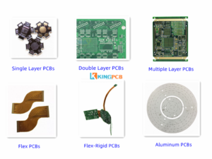
PCB is an abbreviation for printed circuit board. PCB's primary function is to house electronic components and make electrical connections in the electronic components. PCB can be single-layer, double-layer or multi-layer. In 2014, the global bare PCB market exceeded $60.2 billion and expectingto reach $79 billion by 2024.
PCB Types
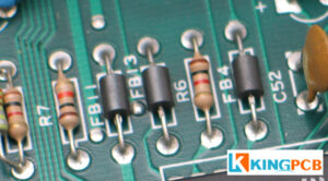
Main PCB Components
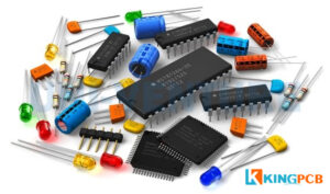
Diode: it allows current to flow in one direction
Lead: light-emitting diode that glows when current flows through it
Resistors: color-coded components that allow current to flow through
Capacitors: design to retain charge for device operation
Switches: allow or prevent the movement of current
Inductors: passive components that resist sudden changes in current
Battery: links voltage to the circuit
PCB Manufacturing Process
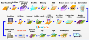
Single-sided process flow
Board cutting → dry film (line) → etching → CCD drilling → solder resist → character → molding → surface finish → electrical testing → final inspection → packaging and shipping
Double-sided process flow
Board cutting→ drilling → sinking copper → board electricity → dry film (line) → lamination → etching → two drilling (some ranked in the solder resist and surface treatment after) → solder resist → character → surface finish (sinking gold some ranked in the character before) → molding → electrical testing → final inspection → packaging shipments
Multi-layer process flow
Board cutting → inner line → browning → pressing → drilling → dross removal → copper sinking → board electricity → dry film (line) → graphic plating → etching → two drilling (some are ranked after anti-soldering and surface treatment) → anti-soldering → character → surface finish (some are ranked before gold sinking) → molding → electrical testing → final inspection → packaging and shipping
PCB Assembly Technology
SMT assembly technology
What is SMT assembly technology? SMT is a method for assembling electronic circuits boards in which components are mounted or placed directly on the top layer of a PCB. Compared to THT, components become smaller and placement of components on both sides of the board. It allowing smaller PCB components with higher circuit density. SMT is ideal for high automation, reducing labor costs, and greatly increasing productivity, and components can be mounted on carrier strips.
THT assembly technology
What is THT technology? THT is the insertion of components with tails or leads into drilled holes in the PCB, also known as feedthrough board assemblies. The leads are then soldered to pads on the bottom of the board, usually using a wave soldering process. THT mounting is very reliable because it creates a strong mechanical bond and the process is relatively mature. Compared to the SMT process, there are fewer variables that may cause solderable problems. The process can make bare boards more expensive due to additional drilling and the potential need to print on both sides of the PCB.
Hybrid PCB assembly
What is hybrid PCB assembly? As electronics tend to be smaller and more functional designs, this places higher demands on PCB assembly. It is challenging to assemble highly complex circuits in a limited space using only SMT or THT, combining SMT and THT technologies with appropriate adaptations to simplify soldering and assembly.
PCB assembly process
Solder paste printing: The first step is to apply solder paste to the board. The printed circuit board and solder stencil are held in place by a mechanical fixture, and the machine applies the paste to the stencil until it covers each opening area evenly.
Pick and Place: Using a mounter that automatically places surface mount components on the PCB. The machine picks up the PCBs with vacuum clamps and moves them to a pick and place station where the PCBs are. Then placed on the workstation and the SMD components are placed on top of the solder paste in the specified location.
Reflow: The circuit boards are transferred via conveyor to a large reflow oven. It heats the solder in the paste at high temperatures to melt the solder. When heating is complete, the board will pass through a series of ovens consisting of cooler heaters, which will help cool and cure the melted solder.
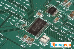
Check: The assembled board should tested functionally to check for bad connections. Common inspection methods include manual inspection, x-ray inspection, and automated optical inspection.
Through-hole component insertion: When the board assembling with other types of components, such as SMT or PTH, you need to use manual welding or wave soldering welding methods to insert PTH components.
Functional test: Functional test is the last step of PCB assembly to test the functionality of the PCBA. The test will simulate PCB operation and monitor the electrical characteristics of the PCB with power and analog signals passing through the PCB.
How to improve the quality of PCB assembly?
Choose proper component size: It is important to choose the correct package size for each component. It is advisable to choose a larger package. That is relatively easier to assemble the entire board again when disassembling and soldering the components.
Design reasonable component footprint: Component footprint is another key consideration for PCB assembly. Furthermore each package is created exactly according to the pad pattern specified in the data sheet for each integrated component.
Design suitable component spacing: Insufficient spacing between components caused by overheating, is one of the main causes of PCB failure. This situation is more obvious in some complex circuits. Redesign and manufacturing will be time-consuming and costly.
Ensure accuracy of the BOM: An error can lead to huge trouble, and manufacturers need to spend a lot of time identifying the problem. When there are new components or replacement, the client should update the BOM sheet in time to ensure its accuracy and validity.
Use of marker points: For use as a point of Mark points are very important for PCB assembly, especially when it comes to close spacing of components.
PCB assembly - KingPCB's services
KingPCB Limited provides complete PCB assembly services. Including PCB manufacturing, component procurement, and assembly. KingPCB's uses the most advanced equipment, with years of experience and stable relationships with electronic component suppliers. We provide the most reliable and highest quality one-stop PCB assembly services to meet the different needs of our customers.
